
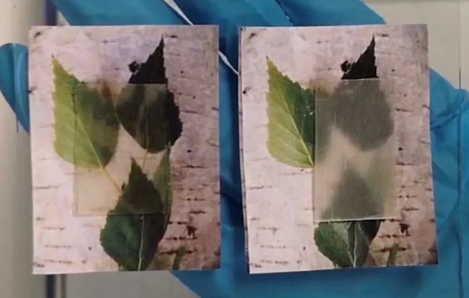
As always when reflecting over a year that is ending, there is good news and there is bad news. We’ll start with the good. A lot of technology is being created. As mentioned last month, new material properties are being created. The one that I find the most fascinating is the creation of transparent wood! This material was developed at the KTH Royal Institute of Technology in Stockholm. [Ref. 1] The wood is capable of both storing heat and being transparent, although the transparency becomes translucent as the heat is released. The figure shows the fully transparent wood on the left and the translucent heat release wood on the right.
In order to manufacture the wood, the researchers took balsa wood and removed its lignin (provides strength and color) and added acrylic into the remaining tissues filling the empty space remaining from the removal of the lignin and hollow spaces that carry water within the tree. This produced the structure that restored the strength lost by the removal of the lignin and provided the optical properties.
Another report [Ref 2] describes increasing the strength of silver conductor by introducing very sight amounts of copper. Their 42% increase in strength is due to their discovery of a new mechanism that works at the nanoscale. They started with the premise that all metals have defects, which leads to undesirable qualities. To compensate for these changes, many have solved that issue by creating alloys to make materials stronger, which tends to reduce electrical conductivity. The team, including researchers from the University of Vermont, Lawrence Livermore National Lab, Ames lab, Los Alamos Nations Lab, and UCLA, began with the fact that as a material size is reduced to the size of a crystal, the material gets stronger. (Hall-Petch relation). This relation no longer holds when the material is in the 10s of nanometers. The boundaries between grains becomes unstable and can move. (Significantly more detail is in the referenced article.) Introduction of copper atoms, which are slightly smaller than silver atoms, allows the copper atoms to move into defect areas in the grain boundaries. The team reported the maximum strength is achieved with boundaries that are 7 nanometers apart.
The future of semiconductors is continuing down the path of continual size reduction. The next release of the Roadmap will provide the requirements for individual structures that will be measured in tenths of nanometers. While that is still years away, the fact that such structures are being contemplated implies the development of equipment that will be able to increase our ability to evaluate phenomena in the single digit nanometer and and below.
There appears to great things happening, so what is the bad news. Unfortunately, the bad news is that the true application of the scientific method is being compromised occasionally. I am not going to pick one specific study. There have been retractions from researchers when others in the field have pointed out that their investigations have produced data that was removed in the final determination of the findings. This is nothing new, but the increase in retractions has been growing since the mid 1990s. [Ref. 3] While the referenced article points out that retractions are not all bad, the increase in fabricated results or falsification has risen along with the rise in retractions. We must have trust in research that is reported.
References:
- https://www.theguardian.com/environment/2019/apr/03/scientists-invent-transparent-wood-in-search-for-eco-friendly-building-material
- https://www.uvm.edu/uvmnews/news/inventing-worlds-strongest-silver
- https://alumni.berkeley.edu/california-magazine/just-in/2016-03-16/retraction-action-science-fraud-more-retractions-could-be