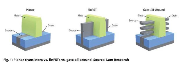
There has been more information in the press about the coming 3nm generation of semiconductors. [Note: I am on the semiconductor roadmap Litho subcommittee. Only information in the public domain will be covered in any of these blogs.) As pointed out in Reference 1,the continual shrinking of the dimensions has required a change in the design of the transistor. There is a selection of the gate all around transistor (GAA) FETs as the most promising direction for the near future devices. This will be a change from the existing finFETs currently in production. At the 3nm or 2nm node the current configuration will cease to be a viable alternative. As mentioned in other blogs, the semiconductor industry will be moving to the 2-D nanosheet transistor. These Gate all Around FETs appear to provide greater performance at lower power. This is a much needed direction. All good things come with consequences. The consequence of the GAA FETs is that they will be more difficult to design and produce, which implies they will be more costly. The picture below (figure 1) is from reference 1 and depicts the evolution of the transistor.

As the designs become complicated and include an increasing number of transistors, the design cost increase. There is an increase cost projected in reference 1. The average design cost for a 28nm chip is $40 Million. A 7nm chip is estimated at $217 M and the cost of a 5nm is $416 M. 3nm is projected to be almost $600Million. The recover of design costs requires very high volume production. There are other designs being considered, but the GAA FET appears to be the most probable.
There is a dark side to the shrinkage of the circuitry. As frequencies increase, geometries get smaller, and voltages decrease, problems can arise. Couplings can occur that the design modeling may miss or not be aware of. Packaging can create its own problems. Coupling or noise can affect the performance of the circuitry. From personal experience, the cause can be surprising. Had a miniaturized design of a special oscillator that was superior to the larger version and easier to manufacture. It was required to be in a shielded container, which was as planned. The circuitry was tested prior to the final assemble and it performed mush better than needed. The container was sealed and the device was dead. Unsealing the container and testing the circuitry demonstrated the device was dead. Repeating the process on two more devices resulted in exactly the same complete failure. The cause of the problem was eventually traced to the packaging. The oscillator required a few inductor coils to achieve the desired performance. Sealing the package placed two of the inductor coils close enough to each other to create a transformer, which spiked the voltage and destroyed the circuit. Once the layer of components was redesigned, the device performed very well. This is just one example of coupling that can create havoc.
Another effect that is increasing in concern is device “aging”. Aging is the effect that shortens the life of the transistor/device. The lower-level effect is based on the pushing the electrons through the transistor channels. Aging has always existed, but the smaller the device dimension, the greater the probability of an impact. Charges being trapped where they don’t belong is a significant cause of the problem. Designs at larger geometries have had more tolerance for these effects. Smaller geometries increase the probability of this becoming an issue. Metal migration is another cause of failure. The dendrites of soldered connections were a significant issue twenty years ago. Currently there are widespread occurrences in high-performance applications like data centers. [Ref. 2] This is a potential problem for the automotive industry. As the dimensions shrink, there will be more engineering challenges that will need to be solved. The improved performance at low power and smaller dimensions will provide the opportunity for many new developments. Working at the nanoscale is introducing new challenges requiring novel solutions.
References:
