Applications based on the properties of new materials

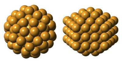
Composites: An interesting set of articles have appeared on composite metal foams.  Research conducted at North Carolina State University (NCSU) by Professor Afsaneh Rabiei [Ref. 1] has developed a material with sufficient properties to stop an armor piercing bullet.  The national Institute of Justice specification is that a bullet be stopped with an indentation of less than 44 mm at the back of the armor.  This particular CMF under an inch thick can stop the bullet with less than an 8 mm indentation at the back.

Metal foams are materials that can be produced by pumping gas through molten metal as it cools.   Cornell University has a different process that places foam into molten metal in a vacuum, where the foam fills the pores within the metal structure.  This material is composed of a soft alloy with a porous silicone foam.  The resultant material is lead free, which opens up many different applications.

The properties of the NCSU composite material is very light weight and appears to have the potential for being employed in nuclear waste storage, since it has some radiation absorbing properties.

Transistors: Applications of graphene transistors have been increasing.  A Japanese research team at Japan’s National Institute for Materials Science designed a graphene field-effect transistor (GFET) consisting of titanium-gold electrons on a single layer graphene deposited in a silicon substrate.  [Ref. 2] The “GFETs can detect harmful genes through DNA hybridization, which occurs when a ‘probe DNA’ combines, of hybridizes, with its complementary ‘target DNA’   Electrical conduction changes in the transistor when hybridization occurs.”

The current procedure detects the DNA hybridization through a labeling of the target with a fluorescent dye, which will shine brightly when it combines with its probe.  This is a complicated and expensive procedure, which also requires expensive laser scanners to detect the fluorescence.  The researchers look to the development of biosensor applications that are focused on genetic disease detection.

Better Magnets through observing Graphene: A system of tri-layer graphene has been has been developed that allows observations of electronic interactions within the three layers of graphene. [Ref. 3] Their work sheds light on magnetism of electrons in three layers of graphene at -272 Celsius and occurs from coordinated weak interactions among many electrons.  Their explanation is that metals have a large density of electrons. Observing the wave nature of elections requires a metal wire of a few atoms wide.  The scattering of atoms occurs in 100nm or less.  Graphene, which has a smaller density of electrons can travel up to 10 microns before scattering.  Observing electrons in graphene between layers for boron nitride provides the ability to observe the electron interactions and the faint “whispers” (as the researchers call it) of electrons interacting with each other.  Understand the interactions will enable the construction of materials with greater interactions.  While they are not projecting future efforts, it is very possible that the understanding of the interaction could lead to the properties required for a material to be a room temperature super conductor.

The developments based on increased understanding of material properties at the nano level can lead to very promising developments in novel material properties.  Stay tuned for more developments in 2017.

References:

  1. https://news.ncsu.edu/2016/04/metal-foam-tough-2016/
  2. https://phys.org/news/2017-02-dna-detecting-transistors.html
  3. http://www.graphene-info.com/tri-layer-graphene-supports-new-type-magnet
Nanotechnology

The State of Nanotechnology

It is always interesting to look forward into the rest of the year.  Nanotechnology will continue to grow and have more applications.  While there is strong and continuing interest in graphene, the application in electronics will continue.  In the semiconductor world, the current focus in on 10 nm, 7 nm, and even 5 nm nodes.  These semiconductor circuits will be based on traditional enhancement of existing device structures and not the application of graphene and carbon nanotube transistors.

The technology advances to work in the “nano” realm have been significant.  The ability to see and measure features at these dimensions have taken science to new concepts.  The ability to see the atomic bonds holding atoms together was accomplished a few years ago.  There is now work being conducted that is able to determine the spin of electrons.  Just recently, Harvard scientists managed to create metallic hydrogen. [Ref. 1]  This was achieved at pressures approaching 500 GPa.  The current thoughts are that the metallic hydrogen will be meta-stable, which should remain when the pressure is removed.  This could open new areas of material science.

In a slightly different area, researchers in Japan are working on evaluating the properties of anti-matter.  The work is done with CERN’s Antiproton Decelerator and the resulting “material” is stored in magnetic bottles. [2]  There is work done by French researchers at CERN to measure properties of antimatter.  Where does this lead?  That will require the development of additional tools.

A term that has been around for a few years is “Atomically Precise Manufacturing”.  The Forbes article [3] provides some insight into advantages and opportunities of APM.  Zyvex Labs is the manager of the Texas based Atomically Precise Manufacturing Consortium. [4]  The long term focus is to work at the atomic scale.  Much of the work in nanotechnology materials development fits into this category.

There are interesting developments in the medical field as biology and nano-sized materials are developed to address various medical conditions.  Imaging of neurons and the interactions have been increasing.  It is quite possible that there will be some breakthroughs on the functioning of the brain that can be used to address “issues of old-age”.  These appear to be conditions where learning what the root causes of the deterioration may indicate means to suppress or even alleviate the effects.  This would provide a double benefit in providing a better quality of life and reducing the impact on medical costs.  This won’t happen quickly, but progress will be made.

Work in superconductors has been working toward a goal of room temperature superconducting material.  Since one of the largest “uses” of electricity is the resistance generated heat of transmission lines, a successful development of material would have the impact of increasing the power generation capacity by much more than 15%.

2017 should be an interesting year with new developments in materials and medicine.  We have many different applications currently in production, but do not have the “one” that everyone needs and can only be supplied by nanotechnology.

References:

  1. http://www.rdmag.com/article/2017/01/first-discovery-atomic-metallic-hydrogen-claimed?et_cid=5803381&et_rid=658352741&type=cta&et_cid=5803381&et_rid=658352741&linkid=content
  2. http://semiengineering.com/manufacturing-bits-jan-24/
  3. http://www.forbes.com/sites/brucedorminey/2013/02/26/nanotechnologys-civilization-changing-revolutionary-next-phase/2/#6a8343d7b95a
  4. http://zyvex.com/
Misc Ramblings, Nanotechnology

2016 Year End Thoughts on Nanotechnology

Without any question, there is a significant amount of research ongoing.  I thought it would be a good time to look back at 2016 and identify progress and/or trends in nanomaterials

Graphene still garners a large amount of published news.  A number of companies are working on various processes to create increased volumes of graphene, others have processes to reduce defects.  Possible applications are being directed at improving batteries through using various layers of graphene.  The possibility exists of creating transistors and compete circuits involving graphene or similar two-dimensional materials.

Applications are still developing, but there is nothing that raises attention indicating there is a significant movement for rapid growth in applications.  Work at Rice is still ongoing to develop stronger concrete, while other efforts are continuing to create materials that heal themselves.  There is the example from a few years ago of the self-healing paint for automobile finishes.  Nothing compares to the initial flurry of activity when carbon nanotubes were incorporated in the bumper of Toyota trucks, or into sports equipment (baseball bats and tennis racquets) to increase strength while decreasing weight.

There have been efforts to develop regulations and governances on the use and applications of nanomaterials.  Europe has been very active in this arena.  While these efforts are moving forward, there have been some discoveries that indicate efforts to define potential problems by size may have some hidden surprises.  Concern over Silver nanoparticles have been highlighted by the toxicity impact on select organisms.  Work done at UCLA [Reference] has shown that the shape of the material can determine the effect.  In this work, plate-shaped nanomaterial appears to be more toxic than wire- or sphere-shaped materials.  [Please note, the word “may” in the work being quoted.]

The issue with a single research effort publication is that it may have experimental errors or other things happening that provide erroneous conclusions.  That is the purpose of the scientific method and the ability of other researchers to duplicate the experiments and arrives at similar results.  When working in new technical areas, they may not be a number of other people working or interested in the same exact area.  Consequently, it takes longer to validate the research.  This is not to indicate that any specific research results are correct or incorrect, only that findings need to be validated by other independent work.

A parting thought for this blog as we start the year 2017: Sometimes, this development process seems to appear to be a repeat of a cycle that civilization has already been through.  There has been a lot of technology/knowledge lost over the centuries.  Current technology is still not capable of creating concrete structures that as durable as the Roman Coliseum.  It is still standing after more than two thousand years.  Our current concrete can not accomplish that feat.  In fact, current technology employs reinforcing steel to strengthen the concrete.  Unfortunately, the concrete containing the metal bars permits moisture to work it way into the concrete.  The moisture then has the capability of oxidizing and eventually destroying the metal employed to strengthen the concrete.  How were the Romans able to develop and apply techniques we do not have today?  How did the artisans in the Middle Ages know how to incorporate certain size gold nanoparticles to create the red coloring in glass?  What else was known and lost through the centuries?

HAPPY NEW YEAR!

References:

http://nanotechweb.org/cws/article/tech/49574

Misc Ramblings

“In-between” Manufacturing

The volume manufacturing of electronics has been around since the early 1900s.  The introduction of the printed wiring (or circuit) board has been the basis of most of the electronic/electrical products since before World War II.  The vacuum tubes permitted the development of circuitry that could add new functionality to the circuitry and enabled the development of radio, radar, and many other advances.  While television was demonstrated int eh 1930s, it wasn’t until the 1950s that it started to become commonplace.

Vacuum tubes had reliability problems with short lifetime and the constant need to replace them.  Banks and banks of vacuum tubes were requi8red for applications and the heat generated by the vacuum tubes and the constant maintenance demonstrated the need for a better solution.  Bell labs developed the transistor to replace the vacuum tubes and increase the reliability of the switching circuits for AT&T’s phone lines.

The development of mass production of the transistor enabled the creation of phone line connections that could automatically route calls to various destinations.  In the early 1960, Texas Instruments (TI) patented the integrated circuit, which enabled the development of more complex circuits with advance functionality.  The semiconductor industry is an outgrowth of these early pioneering efforts.

The semiconductors were applied to various designs for different capabilities.  There was still a need to connect the semiconductors with various functionalities.  This was done by using circuity boards and placing various semiconductor chips into the circuity in the board.

The semiconductor circuitry has grown more complex while the size of the transistor and related components in the semiconductor have decreased.  The doubling of density of components followed a 70% shrinkage in linear size every 18 to 24 months.  (70% width times 70% length yields a 49% area reductions or a doubling of density.)

The semiconductor components are still mounted into individual packages or multi-chip packages, which are them mounted on circuit boards.   The manufacture of  these semiconductor devices requires a package that can be handled by automated assembly equipment.  The limit of circuit board assembly equipment is based on the size of the smallest component that can be picked up and accurately placed.  Current automated electronic assembly equipment is limited to a component no smaller than 0.005 inch (127 µm) by 0.010 inch (254 µm).

Current small devices are in the millimeter range.  Devices smaller than this can be obtained if the volume is very high (in the many millions of devices).  There are examples of devices approaching the single digit millimeter and smaller sizes.  Semiconductors need very high volume to be cost effective for most applications.  The circuit board construction becomes problematic when the sizes shrink to the single digit millimeter and smaller range.  Consequently, it is possible to manufacture devices using circuit boards (or other type of substrates, like thick and thin file substrates).  Semiconductors can be produced effectively in the smaller sizes as long as the volume is large.

There is a gap, sub-millimeter devices, that does not have volume manufacturing capability available for producing quantities of devices that can have various different types of functionality that can be assembled as the mission need changes.  This “in-between” size of manufacturing has not been addressed to date.  There are devices being developed that will require this type of manufacturing capability.  However, the development of this “devices” requires more than a sophisticated assembly mechanism.

This topic will be continued in future blogs.  Stay “tuned”.

Technology

Nano-Safety, Nano-Health Litigations

A report in Reuters dated October 29, 2016 indicated that a woman in California was awarded $70 million in a lawsuit against Johnson & Johnson claiming the company’s baby powder caused her ovarian cancer.  She claimed she had used the J&J product for feminine hygiene for 45 years before she was diagnosed with the cancer per a Los Angeles Times report.  This trial was in St. Louis where two other plaintiffs had awards of $72 million and $55 million.  This initial lawsuit began in 2012 when her daughter saw an ad offering legal representation for people with ovarian cancer who had used talcum powder.

Johnson and Johnson indicated they will appeal the verdict because they are guided by the science, which they state supports the safety of Johnson’s Baby Powder.  They further stated that the Food and Drug Administration concluded in 2014 the such labels were not warranted on cosmetic talc products because the danger is not significant.

In my February 2016 blog, I discussed a case where the family of a dead woman was awarded $73 million from Johnson & Johnson for the supposed cause of her death from ovarian cancer that she attributed to the Baby Powder.  In that case the award was made knowing the facts that the woman may never have used the Johnson & Johnson product and the talc used by the company since the early 1970s has not involved any of the material from locations that have any presence of asbestos, which is a known issue.

So, what are the implications on companies involved in the application of nanotechnology?  How does a start-up survive if every potential product involving nanotechnology might be a potential hazard?  And, whether a real hazard or a dreamed hazard, does every product need to be certified by the FDA?  Although, that did not help Johnson & Johnson.  The issue with this approach is that the full testing and certification can take up to 10 years and cost many millions of dollars.  How does this correlate with the fact that the half-life of a start-up is around 18 months?  The company will perish well before the effect of its material can be determined.  Yes, people will substitute closely related material safety data sheets for new material, but is graphite the same as carbon nanotubes?  No.

To add to these considerations, there has been recent research that has shown it is not only the particle size, but the shape of the particles that has implications.  While the concern over the shape of the carbon nanotubes has been discussed, these new findings indicate that there can be a large number of materials that can have different configurations at given particle sizes.  If this is shown to be true for a number of different particles, it will seriously complicate the research required to evaluate potential health hazards.

So, what is one to do?  That is a very good question.  Unfortunately, each situation will have a unique answer.  Obviously, each company needs to perform due diligence on the materials that are employed and also ensure the workers are protected.  The word-to-the-wise is to be prepared for the unexpected, to document your efforts, and ensure that you are in compliance with Federal guidelines.  That still does not guarantee protection, but it is a very good start.

References: http://www.upi.com/Business_News/2016/10/29/California-woman-awarded-70-million-in-Johnson-Johnson-baby-powder-lawsuit/3191477768102/?spt=sec&or=bn

Nanotechnology Health, Nanotechnology Safety

Applications of Nano

There have been some interesting developments in the application of nanotechnology and related Micro/Nano Electro-Mechanical Systems.  Diabetes has been a growing medical issue/problem for a number of years.  In many cases, the disease becomes fairly advanced before there is any detection of it.  The typical means of detecting the disease is a glucose test, which has required small samples of blood.  Researchers at the University of Houston have developed an interesting twist.  They have developed a non-invasive means of testing by employing a specially designed contact lens that can sample chemicals in tears.

According to their publication [Ref. 1], glucose can be sensed optically though surface-enhanced Raman scattering spectroscopy.  This latest development is created by multiple layers of gold nanowires built on a gold film using solvent-assisted nanotransfer printing.  The device structure is optimized to use the Raman scattering to detect small molecular samples.  The device improves the sensing properties by creating narrow gaps with the nanostructure that intensifies the Raman signal.  At this time there is one caution.  While glucose is present in tears, work needs to be done to develop a correlation with blood glucose levels.

A key element in this work is that being able to monitor chemicals in tears can be the start of creating a device that can monitor various trace chemicals that are linked to a number of physical markers identified and correlated with conditions that require medical treatment or intervention.

There are a number of companies that are developing various medical devices that use micro-channels to sample fluids and provide an analysis of the materials found in almost real-time.  This improved sampling is providing better information for medical personnel at a much more rapid pace that conventional tests.  There is also work being done at various universities that is focusing on novel sensors to provide improved information.

Nanotechnology for cancer treatment has been in the news for years with some significant successes.  The creation of other medical applications could result in significant breakthroughs for many other areas of medicine.

Costs of devices: Nanotechnology is still in the early stages of development.  As the technology matures, there will be a focus on how to reduce costs.  In many cases, this will be the equivalent of comparing apples and oranges.  In the 1980s, the nuclear industry developed a tool for evaluating the representative cost of different approaches to various elements required for power plants.  This technique, Cost of Ownership, was refined by the semiconductor industry in the 1990s in order to evaluate totally different technologies that could be employed.  This is mentioned because it appears that the nanotechnology industry is starting to evaluate some of the manufacturing options.  The evidence for this is the increase in the number of citations of work done in this area in the late 1990s and early 2000s.

A closing note: While the “registration” for this blog site is active, the large number of false registrations has prevented us from approving people for active comments.

References:

  1. http://www.uh.edu/news-events/stories/2016/September/09272016-Researchers-Create-Glucose-Sensing-Contact-Lens.php
Nanotechnology

Manufacturing with “Nano”

There are stages to the development of employing nanotechnology to various devices/products.  It has been an evolution in application and not a revolution. Among the earliest applications that reached the consumer market was the application of Carbon Nano Tubes (CNTs).  From the automotive application, Toyota employed CNTs in epoxies to create light weight and stronger bumpers for vehicles.  The advantage was an increase in strength while providing reduced weight, which translated into better vehicle mileage.  About the same time, Zyvex was instrumental in applying CNTs to sports products like tennis racquets and baseball bats.  Again, the advantage was strength with reduced weight and the ability to withstand greater forces as compared with the traditional products.  This could be considered Stage One in the application of nanotechnology.

There are numerous advances in the medical community.  Gold nanoparticles and CNTs are being developed for the treatment of certain types of cancer.  Researchers in Germany have employed iron-oxide nanoparticles for treatment of brain cancers.  These nanomaterials have been “grafted” on to viruses or similar biological entities that cancer cells consume.  The application of external sources of power to destroy the cancerous cells.  This is a Stage Two effort that incorporates the nanomaterial properties, but is “nano” only because the carrier mechanism is in the nano realm.

Graphene and similar two-dimensional materials have been shown to provide a promising basis for electronics.  CNT transistors have been demonstrated.  There have been two questions on applying these materials.  The first one is the purity or quality of the material.  Graphene tends to have voids in larger sheets, although new research indicates that it might be possible to post-cure the voids that exist.  The question for Stage Three, which is the application of nanomaterials that employ unique properties of the materials in the nano realm, is how does the mass production of these unique structures occur?

Nanomaterials have shown promise, but the applications are still being developed.  The observable exception is the red coloring in the stained glass windows from the Middle Ages and before, which coloring is caused by the inclusion of gold nanoparticles in the glass.

When the need is to use actual nanomaterial structures, the ability to manufacture them is more problematic.  The initial thought is “What about semiconductors?”  Their structures are on the nanometer scale.  That is absolutely correct, but the product is much larger than nanometer-sized devices.  The question is how to we measure, test, and handle nano-scale products/devices?  As an example of this question, consider the following.  If I manufacture 30 nm gold particles, how do I know the distribution of the size?  What is the half-width of the distribution?  Can I use the same method for a gram? a Kilogram? and a ton?  How accurate will the measurements be?  There is still a large amount of significant development that is required before there will be true nanomaterial products.  It is coming, but it is not ready yet.

Nanotechnology

Lithium, Graphene, and batteries

With the reliance of potable electronics on battery power, researchers are exploring various approached to increase the power density of materials for batteries.  The majority of batteries for applications, like cell phones, computers, other portable devices, are based on incorporating Lithium.  More information of the construction of batteries is available in Reference 1 along with other sources available on the web.  The issue is that battery life is too short for most applications and requires frequent recharging during the course of one day.  It was not too many years ago that a trip through an airport had every available outlet being used to recharge some device.  Technology has improved and battery life has lengthened, but the goal is to keep pushing the limits until devices can continue to work for much more than a day without recharging.  There has been a significant amount of research in applying forms of nanocarbon to improve the energy efficiency of batteries.

Over a year ago, there were reports of a graphene technology that will double the life of the Samsung phone batteries. [Ref. 2]  The design is considering replacing the graphite anode with graphene-coated silicon resulting in almost doubling the energy density.  It is expected that it will be several years before the technology finds its way into mainstream products.

Work has been done in improving the efficiency of lithium based batteries to extend the life of devices that rely on portable power.  [Ref. 3] Lithium ion storage is dependent on the structure of the composite materials.  Graphene enters into the picture based on its good conductivity and mechanical strength.  Using carbon nanotubes with the graphene as spacers between layers, resulting in a superior environment for formation of Fe3O4 microshpheres but also maintaining a proper ration and not allowing an overproduction of the microspheres.  Work in China has involved composites that could provide improved performance for lithium-ion batteries.

A recent article is suggesting that a single graphene monolayer could be developed as a support for the electrodes reducing the thickness of the material needed to create the battery. [Ref. 4] The details of the article indicate that anode and cathode are created by electro deposition of zinc and copper on the graphene and are packaged in a graphene based cell. [Ref. 5] This method of generating electrical power, albeit not on the nano scale, goes back at least hundreds of years.

There are other developments that are underway to improve energy storage.  Work is being done on Lithium-sulfur batteries that could have superior energy density to the current lithium-ion batteries. [Ref. 6]  The comparison indicated that the energy density of Lithium-ion batteries is in the range of 130 to 220 Watt-hours per kilogram.  In theory, the Lithium-surfer batteries could be a great as 2,600, which is an order of magnitude greater.

There are continuing developments on the application of graphene to improve the power density of batteries.  A search on “graphene batteries” will turn up links to a number of developments that are currently in process.  This effort is another example of nanotechnology working to improve every day life.

References:

  1. http://www.graphene-info.com/graphene-batteries
  2. http://www.techtimes.com/articles/64353/20150629/samsungs-new-graphene-technology-will-double-life-of-your-lithium-ion-battery.htm
  3. http://nanotechweb.org/cws/article/lab/56969
  4. http://nanotechweb.org/cws/article/lab/65531
  5. http://iopscience.iop.org/article/10.1088/0957-4484/27/29/29LT01
  6. http://cleantechnica.com/2014/12/29/graphene-kill-lithium-ion-batteries/
Electronics

Polymorphism and nano-toxicology

What is polymorphism?  In the Oxford Dictionary, polymorph is an organism or inorganic object or material that takes various forms.  Polymorphism is defined, in material science, as the ability of a material to exist in more than one form of crystal structure. [Ref. 1] A recent publication from Brookhaven National Laboratories that was published in Nature Communications [Ref. 2] reports findings on Gold nanoclusters with 144 atoms.  They were able to find the theoretically predicted icosahedral-cored cluster (left image below) but also found samples with truncated decahedral cores (right image).  The pictures are from R&D Magazine. [Ref. 3]

rd1606_nanoparticle_gold

The researcher, Simon Billinge and his lab, pioneered a method which they call atomic Pair Distribution Function (PDF) to analyze the results of high energy x-ray scattering from the material.  The resulting polymorph provided an explanation of why other researchers have had difficulty in identifying the structure of the material.  The researchers anticipate being able to find additional materials with the polymorphism.

On a different front, there is work being done on impact of environmental exposure to nanomaterials.  Work being done at the Swiss Federal Laboratories for Materials Science and Technology examines an issue of the difference between materials produced for applications and those released in the environment. [Ref. 4]  One example that is described is titanium dioxide.  Adding the nanoparticles to paint a) enhances the self-cleaning capabilities of the paint and b) blocks UV rays thus preventing or diminishing paint degradation. One of the issues is that finding sufficient testable quantities of samples of nanoparticles that have degraded over time is difficult.  This fact makes evaluations of nano-toxicity difficult if not impossible.

Work has been done [Ref. 5] on silver nanoparticles that are added to textiles as biocides to prevent the growth/spread of microorganisms.  There is a release of some of the nanoparticles into the environment.  However, if the released silver ions compline with other ions, like sulphides, they create silver sulphide, which is not an active biocide.  This is part of an over effort to evaluate the life cycle of nanomaterials and will be available in 2017.  More information is available in Reference 6.

An interesting finding is that silver nanoparticle shape affects its toxicity. [Ref. 7]  Research was done on the impact of silver nanoparticles shape (spheres, rods, and plates) on rainbow trout cells and zebrafish embryos.  The researchers concluded that the silver nanoplates induced oxidative stress in the cells through the production of superoxides, which are toxic.  There were conditions that they placed on the experiments and will require further and expanded testing.

This brings us back to the title of this blog.  If nanomaterials can have different shapes/configuration, then the potential results of toxicological investigations will depend on the shape of the material.  If the material has the ability to shape-shift, how do we develop testing methodologies that account for the possible difference impact of the material shapes.  If you think that the shape does not make a difference, I will give you two pounds of graphite (carbon) for one pound of diamond (carbon).

The evaluation of the environmental/human impact of any nanomaterial must incorporate the fact that these materials have properties based on the shape under test and not an overall classification of material size.

References:

  1. https://en.wikipedia.org/wiki/Polymorphism_(materials_science)
  2. http://www.nature.com/ncomms/2016/160614/ncomms11859/pdf/ncomms11859.pdf
  3. http://www.rdmag.com/news/2016/06/gold-nanocluster-discovery-hints-other-shape-changing-particles?et_cid=5351098&et_rid=658352741&type=headline&et_cid=5351098&et_rid=658352741&linkid=http%3a%2f%2fwww.rdmag.com%2fnews%2f2016%2f06%2fgold-nanocluster-discovery-hints-other-shape-changing-particles%3fet_cid%3d5351098%26et_rid%3d%%subscriberid%%%26type%3dheadline
  4. http://nanotechweb.org/cws/article/tech/65333
  5. http://www.ncbi.nlm.nih.gov/pubmed/24941455
  6. http://iopscience.iop.org/journal/0957-4484/page/Focus-Lifecycle-of-nanomaterials
  7. http://nanotechweb.org/cws/article/tech/49574


Nanotechnology Health

Is it Time for 3D Printed Food?

Why would you consider 3D printed food to be in the realm of nanotechnology?  Nanotechnology involves the usage of particles that are well below what we would consider required for food.  This is true.  In a previous blog, the work done on developing current food types are very large.  Most 3D printers are hard pressed to be accurate within a few microns, much less nanometers.

Before covering the need for nanotechnology, a review of existing equipment is useful  3D Systems [Ref. 1] has information on their Culinary Lab where experiments are being conducted on developing food the is both tasty and beneficial.  There is a web site [Ref. 2] that has a listing with examples of various types of food printers.  There was a 3D Food Printing Conference [Ref. 3] held in April 2016 in The Netherlands that addressed many aspects of food printing.  Most of the efforts currently are on producing exotic designs in the food.  There is mention of customized cakes of personalized desserts that are being commercially produced.  But, this is not a food benefit of 3D printing but a design benefit.

In a previous blog where I mentioned the Star Trek food replicator, the work being done today for NASA is directed at being able to supply food on deep-space missions.  When one considers the amount of food that would be required to support three people on an eighteen month round trip, the room required to store the food and the space to preserve and store it are not only large, but very expensive to lift out of earth’s orbit.   A demonstration of a 3D printer for food was demonstrated at a recent South by Southwest in Austin.  The startup, BeeHex, is working on converting dehydrated food particles into food with both flavor and texture. [Ref. 4]

One advantage of 3D printing of food is that it should be possible to supply nutritious food to people in very remote parts of the world.  One of the problems that exist today is that a significant potion of the food grown spoils before it reaches its intended market.  If the constituent parts could be shipped safely with danger of spoiling and then reconstituted into nutritious food, some of the hunger problem in the world would be addressed.  The European Union has a program called PERFORMANCE (Development of Personalized food using Rapid Manufacturing for the Nutrition of elderly consumers). [Ref. 5] This approach permits the addition of various nutrients needed by the person who the food is created for.  This was demonstrated in a conference in Brussels in October 2015.

NASA has a definite interest in developing this ability.  There was an SBIR award to an Austin, Texas company to begin the development of creating unflavored macronutrients, i.e., protein, starch and fat, the sustenance part of a required diet can be quickly produced in numerous shapes and textures from a 3D printer with heating capabilities. [Ref. 7]

This technique is also being investigated by various military organizations as a means of delivering quality meals in the field.  While the “Foodini” will only produce products made of dough, paste, of high viscosity liquids, this is the start of possible home appliances. [Ref. 8] The microwave comes to mind as a once expensive piece of equipment that is now common in many homes.

So where does the nano come into this picture?  The basic concepts of both handling food and handling nanomaterials come together.  Some of the materials will probably contain nanoparticles is a predefined portion to the entire volume.  This requires method of inspection and verification that currently are not defined.   There will need to be very specific procedures developed to ensure the proper mix of ingredients.  At this time, one can only guess one the various sizes will be required, but for many of the foods, printing very thin layers rapidly will be needed to create tasty and nutritious meals.  bon appétit!

References:

  1. http://www.3dsystems.com/es/culinary
  2. http://www.3ders.org/articles/20151102-3ders-monday-warm-up-the-top-3d-food-printers-that-will-feed-the-future.html
  3. http://3dfoodprintingconference.com/
  4. Austin American Statesman, April 22, 2016 edition, Tech Extra section, Page SA2.
  5. http://3dprinting.com/food/from-puree-to-3d-the-eu-performance-project-presents-results/
  6. https://www.naturalmachines.com/
  7. http://sbir.gsfc.nasa.gov/SBIR/abstracts/12/sbir/phase1/SBIR-12-1-H12.04-9357.html?solicitationId=SBIR_12_P1
  8. http://3dprinting.com/food/us-army-might-use-food-printers-future/


Misc Ramblings, Nanotechnology