Blog currently under revision and reference check.
References:

Blog currently under revision and reference check.
References:
There is an indication of the need for additional workers in the technical Workforce. SEMI [Ref. 1] has indicated there is a shortage of 80,000 to 100,000 semiconductor workers. With the surge in creating additional semiconductor fabs that number is sure to grow. The growing Space industry is also in need of trained workers. The same can be said of the med-bio industry. We don’t have the quantity of skilled workers, so where do we get them. Part of the solution is to recognize that we, ourselves, have created the problem.
In the early days of the semiconductor industry, almost all the positions within the actual manufacturing facility or called the fabrication (fab) facility had challenging procedures with exotic equipment. A mistake or an unexpected variance at any one of hundreds of steps could result in unusable devices. The solution was to use highly skilled personnel, usually people with PhDs is very specialized areas. As the functions increased on the devices, more steps were introduced, which could provide for more failure points. The solution was to employ more highly skilled people. With a typical education cycle for a technical PhD of 5 or more years, the supply of the needed personnel was not sufficient. So, the solution was to consider a way of finding “less trained” personnel, who have “only” one or two Master’s degrees.
There are organizations that are trying to address this shortage, but the solution is not as simple as one would think and is also simpler than one imagines. The basic question that needs to be addressed is what skills are really needed. Using an example from more than fifty years ago. If one needed a mechanic to work on vehicle transmissions, it was necessary to understand want was involved in stick shifts, which were manual transmissions. The “automatic” transmissions were the exception. So knowledge of the manual transmissions were a very important part of the job description.
What has happened in the semiconductor industry? One could say that the equipment has improved significantly, which is true. But a key factor is that the recipes for the manufacture of the devices have stabilized and involve less constant tweaking. As the process stabilizes, the need for the higher levels of education is reduced. Jobs that could only be performed by PhDs, now can be run by techs with less formal education but a better understanding of the minor changes required to keep the process variable under control. But, have the educational requirements been modified to reflect the increased sophistication of the equipment and process controls?
There is another factor in the fact that each company employs different equipment and variations of the recipes. Consequently, the “learning” in a structured course will most likely need to be implemented with additional courses/training at the specific company. So, what is the best way to obtain the desired workforce. There are three approaches, which also require an understanding of what level of education and understanding is required.
The first is to create a general program that address the needs across an entire industry wherever the work will be accomplished. This program provides the basics and is typical of programs like the SEMI Workforce efforts [Ref. 2} or the Texas State University Round Rock Campus program, which covers multiple different fields in the area beyond semiconductors. The issue is that the individual companies may find a lot of what is covered and not applicable to their specific interests. They will gladly hire the individual and retrain them to meet their internal needs.
The second approach is to bring a training program inside the organization. This may work for very large companies that can afford either to bring new employees to a central location for training or for the company to have multiple locations that train their new hires. This requires an internal organization and the hiring of an external organization that specializes in their technology. The advantage is that the new workers are learning on the exact equipment they will be using in their day-to-day duties.
The third option is best explained by an example that has succeeded in Minnesota. Employing a concept that has been fully developed by Newberry Technology Associates [Ref. 3], the nanotechnology needs of the local industry were investigated and an educational program developed to train the technical graduates from the Dakota County Technical College to have skill matched to the industry needs. This 72-credit program [Ref. 4] was a success and has won awards for its accomplishments thanks to Newberry Technology Associates’ development and oversight.
There are choices to address the workforce needs and the effort and direction is dependent on the specific situation. Each company and local needs to determine the best way forward to satisfy the needs of the specific location. This applies to any industry whether semiconductors, aerospace, med-bio, or a new developing industry. Chose wisely for the best path but investigate previous successes for guidance.
References:
There are times when there is an established technology that undergoes a modification. There are also times when different technology approaches compete. In the early days of distributed electricity, Direct Current (DC) came to forefront. It was understood and built on knowledge from working with various types of sources, some of which we variations of the battery. Alternating Current (AC) had a more complex insertion into every day life due to the fact, that AC did not have the mathematics that would enable the creation of a supply system for AC power. Nikola Tesla created the ideas and the rationale on how to develop the AC system in existence. Reference 1 provides a background on Nikola Tesla.
The first automobile, which was gasoline powered, was patented by Carl Benz [Ref. 2]. The first electric power vehicle ran using a lead-acid battery and was introduced in 1888 [Ref. 3]. The first steam powered automobile was introduced in 1769. The vehicles were restricted to people with significant funds, until Henry Ford created the mass assembly line. By this time, the ability to have fuel sources accessible and the reliability of the vehicle power system created the use of the gasoline engine.
We have two similar situations that involve sources of energy. The current growth in demand for electrical power to drive both cloud storage farms and provide enough energy for the genAI computational efforts are straining the existing energy system. The other challenge is the electric vehicles and their need for energy but require a substantial time to refill the depleted batteries.
The sources of energy are mentioned first, because without that source, batteries can not be replenished. If one considers the various types of environmentally friendly operation, there are four types. Solar uses the energy from the sun and creates DC, which can be converted to AC. Wind power employs capturing energy from wind moving a turbine to generate electricity. Hydro power (dams) use the natural flow of water in a river or other stream of water, to turn turbines to create electricity.
Of these four types, there are only two that are continuous, water and nuclear. Granted that water generation does require the stream to be flowing. There was the completion of a new nuclear power plant in Georgia [Ref. 5]. As has been the history of nuclear power, the cost overrun and time delay from the original estimate. This power plant is capable of continuously supplying enough power for 500,000 homes for 60 to 80 years. One issue is that it takes too long to obtain all the permits and actually build a plant.
A different type of nuclear reactor is being developed and are called Small Modular Reactors (SMRs) [Ref. 6]. The advantages the SMRs are many in the fact the unit is smaller, has the ability be to located in smaller areas, can be linked with adjacent reactors to increase power, and can have much of the construction done separately. Currently, there are more than 80 of these type units being developed in countries around the world. There are also other types of nuclear reactors being developed from research accomplished in the 1980s.
That still leaves the issue of energy storage once it is received. Much work has been done on Lithium based batteries. Various chemical compositions are being investigated to reduce the current issue with Lithium based batteries. One large disadvantage is the time to recharge the batteries. There is an alternate storage material being investigated: iron-air batteries [Ref. 7]. The advantage of the iron-air battery is that it can have a slow discharge of days. That provides the potential for employing this type of battery to capture solar and wind generated power and keep it stored for days, which Lithium based batteries can not. Iron is heavy and seems to indicate that the most favorable application would be stationary power storage. Weight aside, the iron-air battery can be recharged with much higher power levels than other types of batteries. Is this another evolution similar to DC to AC?
References:
Last year, the November blog mentioned some of the challenges with Generative Artificial Intelligence (genAI). The tools that are becoming available still need to learn from some existing material. It was mentioned that the tools can create imaginary references or have other types of “hallucinations”. Reference 1 quote the results from a Standford study that made mistakes 75% of the time involving legal matters. They stated: “in a task measuring the precedential relationship between two different [court] cases, most LLMs do no better than random guessing.” The contention is that the Large Language Models (LLM) are trained by fallible humans. It further states the larger the data they have available, the more random or conjectural their answer become. The authors argue for a formal set of rules that would be employed by the developers of the tools.
Reference 2, states that one must understand the limitations of AI and its potential faults. Basically the guidance is to not only know the type of answer you ae expecting, but to also evaluate obtaining the answer through a similar but different approach, or to use a competing tool to verify the potential accuracy of the initial answer provided. From Reference 1, organizations need to beware of the limits of LLM with respect to hallucination, accuracy, explainability, reliability, and efficiency. What was not stated is the specific question needs to carefully drafted to focus on the type of solution desired.
Reference 3 addresses the data requirement. Depending on the type of data, structured or unstructured, depends on how the information. The reference also employes the term derived data, which is data that is developed from elsewhere and formulated into the desired structure/answers. The data needs to be organized (formed) into a useful structure for the program to use it efficiently. Since the application of AI within an organization, the growth can and probably will be rapid. In order to manage the potential failures, the suggestion is to employ a modular structure to enable isolating potential areas of issues that can be more easily address in a modular structure.
Reference 4 warns of the potential of “data poisoning”. “Data Poisoning” is the term employed when incorrect of misleading information is incorporated into the model’s training. This is a potential due to the large amounts of data that are incorporated into the training of a model. The base of this concern is that many models are trained on open-web information. It is difficult to spot malicious data when the sources are spread far and wide over the internet and can originate anywhere in the world. There is a call for legislation to oversee the development of the models. But, how does legislation prevent an unwanted insertion of data by an unknown programmer? With out a verification of the accuracy of the sources of data, can it be trusted?
There are suggestions that there needs to be tools developed that can backtrack the output of the AI tool to evaluate the steps that might have been taken that could lead to errors. The issue that becomes the limiting factor is the power consumption of the current and projected future AI computational requirements. There is not enough power available to meet the projected needs. If there is another layer built on top of that for checking the initial results, the power requirement increases even faster. The systems in place can not provide the projected power demands of AI. [Ref. 5] The sources for the anticipated power have not been identified mush less have a projected data of when the power would be available. This should produce an interesting collusion of the desire for more computer power and the ability of countries to supply the needed levels of power.
References:
The term meta-materials refers to materials that are created by producing material structures that do not occur in nature and also can be created with structural complexity that also would not occur in nature. Graphene has long been a material of interest. For a long time, the issue with graphene has been the ability to produce it in large areas without any defects. The work done in Reference 1 was focused on evaluating a nano electronics platform based on graphene. The interest is because the technology is compatible with conventional semiconductor manufacturing. This work was based on the results of research that found a layer of graphene formed on the top of silicon carbide crystal. It was discovered that electric currents flow without resistance along the edges of this material plus the graphene devices could be interconnected without metal wires. The researchers observed that the electrons could travel over large distances, microns, without scattering. Previous technologies could only obtain 10 nm before scattering. Their estimates are that it will be up to 10 years before the graphene-based electronics could be realized in volume manufacturing.
A slightly different class of two-dimensional meta-materials is called MXenes. These MXenes are part of a large family of nitrides and carbides of transition materials constructed in two dimensional layers where two or more of the metal layers are interspersed by a carbon or nitrogen layer. This surface is finished off with a termination layer. According to the researchers [Reference 2], these MXenes can be fabricated as nanometer thin flakes that can be better dispersed in water and inked onto any surface. They can also be made as films, fibers and even powders research areas using these materials includes optoelectronics, electromagnetic interference shielding, wireless antennas, total catalyst, water purification, biosensing, and many more. There is also the possibility of using these materials as alternatives to lithium-ion batteries. The issue right now is that this material tends to oxidize and degrade quickly in ambient operating conditions. Removing the oxidation will require some additional inventions. Work done in Australia has found one method to work to remove the oxidation, which focuses a 10 MHz frequency beam, which breaks the bond of the oxidation. Some work in China has use this material as an electrochemical biosensor that is coupled with gold nano arrays to attempt to have a noninvasive cancer detection system. One of the challenges using this material is that there are an extremely large number of possible configurations. Finding the best ones to work with will require significant computational analysis.
Reference 3 looks at a new layering technique for two dimensional materials with the possibility of being able to tune the materials for different applications. One of the findings was that sandwiching atomic layers of a transition metal like titanium between monoatomic layers of another metal, like molybdenum, and using carbon atoms to hold them together. The researchers discovered that a stable material can be produced. A key result of their work which could be beneficial in the future is that they have found a way to combine elemental materials into a stable compound, which will exhibit new properties. This particular arrangement of atomic structures opens up the possibility to fine tune the resulting molecular structure and its related physical properties to meet certain stringent applications that at the present time cannot be considered.
The development of the atomic layer materials and the ability to manipulate them into ways that produce different characteristics is opening up an entirely new world for researchers to create new, and previously unknown, material properties. This is not something that will happen immediately but the effort is providing a whole new branch of scientific experimentation. It will be interesting to see what the future brings.
References:
Over the years, we have witnessed the issues or multiple peer-reviewed papers being recalled. A recent example as reported in numerous places, Reference 1 states: “The Dana-Farber Cancer Institute (SCFI), an affiliate of Harvard Medical School, is seeking to retract six scientific studies and correct 31 others that were published by the institute’s top researchers, including its CEO. The researchers are accused of manipulating data images with simple methods, primarily with copy-and-paste in image editing software, such as Adobe Photoshop.”
There were allegations of data manipulation in 57 SFCI-led studies. [Ref. 2] There has been an increase in the application of AI applications being employed to check for fraudulent imagery. In an editorial [Ref. 3] in Science, they assert that they are using Proofig to look for image duplication or other types of image modifications. They also employ iThenticate for plagiarism detection.
In a related area, AI is running into copyright difficulty with its generated images. The IEEE Spectrum magazine [Ref. 4] has an article on the potential for copyright violations. One example shows a generated article almost 90% identical in words and sentences from a New Youk Times article. While this article references this type of result to plagiaristic outputs, it is plagiarism if a person did that. The ability of AI generated texts to create imaginary references has been referenced as having hallucinatory output. A key question that was generated was: is there any way for a user of the generative AI to ensure there is not copyright infringement or plagiarism? A good question that will need to be answered. In the evaluation of images, the researchers found hundreds of instances where there was very little difference for recognizable characters in video and games. This analysis was based on a very limited study of subjects (a few hundred).
While the use of Generative AI is becoming more widespread, even careful reviews of the data and pictures will not prevent the misuse of the results. In the April 2020 Blog [Ref. 5] the topic of scientific integrity and COVID-19 was covered in detail. The key points were that even with a solid research foundation the results can be subject to misinterpretation by people who are unfamiliar with various techniques of analyzing the data. Another point in that blog is that when the results of an analysis are reduced to a single number, the potential for creating inappropriate impressions is high. So, the construct of the model and the assumptions are very important.
This brings up another question of what are the under pinnings of Artificial Intelligence programs. What are the algorithms that are being employed AND do these algorithms interact with each other. As described in earlier blogs involving expert systems work in the 1980s, the expert system is based on the environment (data analyzed) it was created for. The expert systems then improved its performance based on the new data acquired though its operation. This is a problem of self-biasing. AI programs are built on a base of information. Sometimes the data absorbed is protected, e.g., the New York Times database. So, all the data might not be available. If one were to focus on a single database and develop that for projecting future information, there would be significant difference in news projection depending on if the data were obtained from CNN or Fox News.
The applications and even the development of new tools for creating reports and the complementary programs for evaluating the veracity of the information presented are still in the very early stages of development. This year, 2024, should witness some interesting development in the application of AI tools. Significant assist in medicine is being provided already and more should be coming. It just requires careful application of the programs and understanding the data.
References:
The most popular technical/computer topic at the end of 2023 was Generative Artificial Intelligence (AI), which was briefly touched on in last month’s blog. As 2023 draws to a close, the New York Times is suing the major developers of Generative AI for using their copyrighted news database without permission or compensation. [Ref. 1] On the restrictive side, the UK’s top court decided that AI can not be named as an inventor on a patent. [Ref. 2] It also indicated that the person who owned the program results was not the owner of the patent, because he was not named on the patent application as inventor. This should make for an interesting upcoming year and patent law.
Regarding materials and semiconductors, there is a proposed new approach to semiconductor material. Ferroelectric semiconductors are being studied. The issues of speed, size including thickness (or thinness) and operation at high speed and high power are a challenge for moving into larger, bigger, faster devices. The University of Michigan research [Ref. 3] is focused on ferroelectric high electron mobility transistor (FeHEMT). Ferroelectric semiconductors can sustain an electrical polarization, think magnetism. But, the ferroelectric semiconductor can switch which end is positive and which is negative. In other words, the transistor can change how it functions.
Researchers at Lund University in Sweden [Ref. 4] have shown a configurable transistor. The potential for this device is a more precise control of the electronics. Their work is with III-V materials to replace silicon. The promise is high-frequency applications (6G and 7G networks) while reducing the power required. The application would significantly benefit neuromorphic computations, which would enable stronger AI applications. They examined new ferroelectric memory with tunnel barriers in order to create new circuit architectures (transistor type memory). A key part of this work is the creation and placement of ferroelectric grains in the device structure. This is a ferro-TFET transistor. Like the development mentioned above, the properties of the transistor can be modified during the operation of the device. One advantage is the “new” properties of the device remain constant even without any power needed to keep their state.
Researchers from Northwestern University, Boston College, and MIT are pursuing a different type of transistor function. [Ref. 5] They claim it can store and process information simultaneously, like the human brain. A key difference form previous research is that the focus is bringing the memory and processing functions together without the necessary time lag of transporting the electrical signals. Their claim is that by layering different patterns, two dimensional materials are formed that have novel properties from the individual materials. The researchers stacked bilayer graphene and hexagonal boron nitride. By rotating one layer with respect to the other, different properties could be developed in each graphene layer. One lead researcher introduced a new nanoelectronic device that appears to be capable of manipulating data in an energy efficient manner. In their experiment, that have demonstrated their synaptic transistor can identify similar patterns. The additional claim is that the new device can provide a major step forward in AI applications.
It appears that the work on novel transistor structures and functionality might provide higher frequency applications with the potential of reducing the total power requires. The power reduction directly effects the reduction of the heat generated by the devices. We can expect more results in the coming 2024 year.
References:
Artificial Inelegance (AI) seems to be in the news with promises of a tremendous amount of benefits for the average person. Specifically, “Generative AI” will be the foundation of all these benefits. Before we start believing all the super benefits from Generative AI programs like ChatGPT, it is instrumental to understand the background behind these newer programs.
In the early 1980s, personal computers started becoming a tool that was adopted by large businesses. The development of spreadsheet programs, like SuperCalc, provided the ability to analyze large amounts of data that would have required many weeks of effort from many people. It was simple to create a database so that one that could store, modify, and analyze data in vast amounts that were not possible previously.
The next step was the ability to create a program with self-learning, an expert system. The earliest ones were simple. One could develop a system that evaluated results and then make predictions on what the possible cause was or provide guidance for a future outcome. One of the first ones, the author developed was an analysis of quality failures from a manufacturing facility. There was a history of failures in the final testing and related causes that had been previously identified. Once the system was in place, future identified failures would be identified along with the cause and that data entered into the database. Over time, the ability to predict the cause of failures would become more accurate due to the additional data being entered. This type of expert system has a built-in trap!
What is the trap? When the data is being collected from one location it will be applicable to that specific location and may not even apply to a different location. As an example, consider a set of identical twins. If one goes to a high school that focuses on science and technology, and the other goes to a high school that focuses on artistic talents, like acting or music, the twins will have different capabilities when they graduate. The area that the learning occurs in impacts the end result. The trap is assuming that the expert system can apply across everything, which it is specifically focused.
In the latter part of the 1990s, Text Mining was developed to analyze and correlate relations among documents based on occurrence of text phrases. Based on the phrases, it was possible to develop the frequency of occurrences between other items in the documents. Based on the identified frequencies, it is possible to predict correlations among items identified in the original text analysis. This provided the program builders with a means of pulling specific content from existing documents.
While most people don’t realize it, ChatBots have been around for more than ten years. What is a ChatBot? It is a computer program that can simulate a conversation with a person. These started as simple question and answer communications with the ability to either speak your answer of enter something from a keyboard. As additional decision making was added (i.e., artificial intelligence) to assist the person through a selection of choices. “The latest evolution of AI chatbots, often referred to as “intelligent virtual assistants” or “virtual agents,” can not only understand free-flowing conversation through use of sophisticated language models, but even automate relevant tasks.” [Ref. 1]
This brings us to the latest efforts that are known as Generative AI, which can pull from a vast amount of date to produce text, images, videos, etc., that appears to be original concepts. Yes, the information that is provide may appear to be novel, but it is based on a collection of existing data and an algorithm(s) that control how the computer directs the accumulation of data and in what manner the results are presented. There is a concern that the control of the algorithms provides the ability of what type of results will be provided. An article in the November 30, 2023 issue of the Wall Street Journal provides an argument for these algorithms to be open source and available to all. [Ref. 2]
That bring us to the title of this blog. If one considers the computational power available, the analysis of multiple combinations of molecules based on a predetermined set of characteristics can be employed to eliminate a lot of possible combination and provide some strong suggestions for researchers to evaluate. The program is building on historical data and algorithms to do its specific analysis. The same type of effort can be applied to novel combinations of materials/elements. With whatever guidelines are incorporated in the algorithms, the results can provide novel materials. Some would say the computer “created” the new drugs, materials, or whatever. In reality, the results were created by the people who created the algorithms – human input and human direction. This raises an interesting question. Are the people who created the algorithms the real owners of the “discoveries”? Something for the courts to decide in the future.
References:
Today’s electronics are based on the transistor, which can be switched either on (a one) or off (a zero). Among other things, the sounds coming from musical instruments are basically smooth variations, which are described as analog signals. In order for the signals (electronic representations of the sound waves) to be processed, there must be a conversion from the analog wave to a digital representation of the original wave. An analog to digital converter continuously transforms analog signals into the binary (ones and zeros) equivalent at each instant of measurement that can be processed by the electronic equipment.
Consider the piano and violin representation of their frequencies between C and B (twelve notes) on a piano. Figure 1 shows the 12 notes from C through B, with the A being the key frequency of 440 Hz. [Re. 1] The point of this chart is to present the fact that the piano has fixed notes and is more like digital information from a computer. The violin, on the other hand would provide a continuous range of the various frequencies. (There is also a slight variation of the piano key frequencies from a straight line for the violin.)
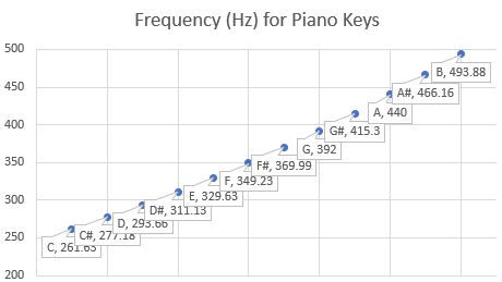
Figure 1
One interesting item is that since the piano has discrete frequencies associated with the various keys, the actual sound is not a smooth ramp up and down like a sine wave.
Figure Two depicts a violin and a piano note and shows the rapid drop-off of the note from the violin. [Ref. 2]
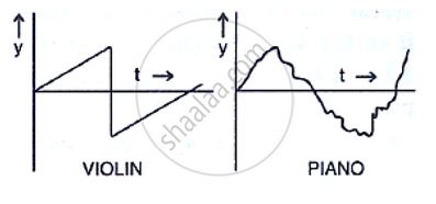
Figure 2
The piano note is created by the key striking the stretched piano wire that has been properly tuned. The initial strike is full of non-harmonic tones that dampen down rapidly. [Ref. 3] This reverberation from the strike produces the wave form. The violin is different in that the vibrating string creates harmonics that create the multitude of peaks and valleys shown in Figure 3 [Ref. 4].
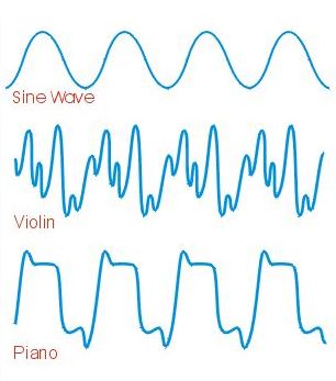
Figure 3
I will borrow some explanation of harmonics from reference 5. It explains that the instrument produces different wave shapes based on the shape of the instrument. that demonstrate comparison of wave shape and harmonics. Another factor is the way the note is played. “If you press a piano key and release it, the sound changes volume gradually over time. First, it rises quickly (or “attacks”) to its maximum volume. Next, the sound “decays” to a lower level and stays there or “sustains.” Finally, when we let go of the key, the sound “releases” and dies down to silence.”
” There are other factors too. An instrument doesn’t just produce a single sound wave at a single pitch (frequency). Even if it’s playing a steady note, it’s making many different sound waves at once: it makes one note (called a fundamental frequency or first harmonic) and lots of higher, related notes called harmonics or overtones. The frequency of each harmonic is a multiple of the fundamental frequency. So, if the fundamental frequency (also called the first harmonic) is 200Hz (which we can think of as simply 1 × 200Hz), the second harmonic is 400Hz (2 × 200Hz), the third is 600Hz (3 × 200Hz), the fourth is 800Hz (4 × 200Hz), and so on. Playing together, the harmonics make a dense, complex sound a bit like a barber’s shop choir, with low voices and high voices all singing in tune. The more harmonics there are, the richer the sound.”
Getting back to Analog and Digital, what the instrument is delivering is a continues series of complex waves that include small and smaller portions of the waves. Taking these waves and “chopping” them up into discrete segments has to average out the variation in each of the measurement size chunks of sound waves. So, no matter how fine one dissects the wave, there is averaging with each bite-sized piece of the actual music. It is possible to take that measurement down to a small enough size that the typical listener will not notice the subtle differences from the analog. BUT, sound can also be subtly felt. No matter how small the averaging size, there will be a difference from the original analog sound wave. Consequently, vinyl (records) is making a come back due to the superior reproduction of actual sounds due to vinyl being an analog delivery of the sounds.
References:
There is no question that we live in a digital world. What does that mean? Is there another world? What is the difference? We live in a world of computers. Computers are based on components of electrical circuits. The basic part of the circuit is defined by either being “on” (conducting electrical signals) or “off” (not conducting). Each of these basic circuit parts in considered a “bit”. So, a 32 bit controller divides the control in to 32 steps, while a 64 bit has 64 steps. Notice, the term “steps”. If one considers a child’s slide, it is a continuous slope. If we were to make that digital, it would have small steps in place of the continuous slide. We would not do that, of course. But we do that with electronics. Have you ever tried to adjust the volume from a speaker and found one setting was too much and next lower setting was too little? That is due to the digital steps in the controller. It is possible to increase the steps to make it appear to be smooth, but it would still be steps.
From Reference 1: “An analog computer or analogue computer is a type of computer that uses the continuous variation aspect of physical phenomena such as electrical, mechanical, or hydraulic quantities (analog signals) to model the problem being solved. In contrast, digital computers represent varying quantities symbolically and by discrete values of both time and amplitude (digital signals).” Analog computers were used in the 1940 to provide assistance with fire control weapons systems during World War II among other applications.
The digital computer became the standard for multiple reasons. The speed of calculation became greater and greater than analog computers. There was one fundamental issue that hindered the application of analog computers. Reprogramming was accomplished by rearranging the interconnecting wires/cables within the assembly. Digital computers in the early days had basic system instructions (neumonic identifiers) that were entered into the computer via numerical codes. This was slow but faster than rewiring the system. When the operating systems emerged for digital computers, the computer could perform a multitude of tasks and not be designed for specific problems.
If digital is faster (and better?) than analog, why are people going back to vinyl records? Why do these people state that the quality of the music is better? Vinyl records are made by equipment that records the actual frequencies as analog signals into to a master copy that captures the nuances of the changes in frequencies. This implies that the equipment can record the analog signals, which implies a system with vacuum tubes and not computer-generated analog to digital converters. To obtain the true effect of the music to be similar to being at and actual performance (not amplified by digital equipment) requires the equipment playing the sounds is also capable of producing analog signals with out electronic digital to analog conversion.
In a very crude example. A piano key strikes a chord that vibrates at a given frequency. The key next to it is at a known, discrete frequency. E.g., the middle C of a piano is 261.6 HZ, the black key to the right has a frequency of 277.18 Hz. This is not continuous as it would be for an instrument like a violin. The piano is the digital instrument (discrete bits) and the violin is the analog (continuous frequencies). The recording in Reference 2 was done during a practice session by “eg” and has both piano and violin music. The quality of the recording is not very good, but the differences between the piano (digital) sound and the violin (analog) sounds are obvious. This example was recorded in an auditorium with a small voice recorder, which was digital. The point is there is a recognizable difference between the analog and digital type sounds.
Next month, Part II will delve into some of the subtleties of employing digitally modified analog signal along with more on sound itself. The modification does not come without consequences.
References: