Today’s electronics are based on the transistor, which can be switched either on (a one) or off (a zero). Among other things, the sounds coming from musical instruments are basically smooth variations, which are described as analog signals. In order for the signals (electronic representations of the sound waves) to be processed, there must be a conversion from the analog wave to a digital representation of the original wave. An analog to digital converter continuously transforms analog signals into the binary (ones and zeros) equivalent at each instant of measurement that can be processed by the electronic equipment.
Consider the piano and violin representation of their frequencies between C and B (twelve notes) on a piano. Figure 1 shows the 12 notes from C through B, with the A being the key frequency of 440 Hz. [Re. 1] The point of this chart is to present the fact that the piano has fixed notes and is more like digital information from a computer. The violin, on the other hand would provide a continuous range of the various frequencies. (There is also a slight variation of the piano key frequencies from a straight line for the violin.)
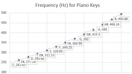
Figure 1
One interesting item is that since the piano has discrete frequencies associated with the various keys, the actual sound is not a smooth ramp up and down like a sine wave.
Figure Two depicts a violin and a piano note and shows the rapid drop-off of the note from the violin. [Ref. 2]
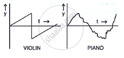
Figure 2
The piano note is created by the key striking the stretched piano wire that has been properly tuned. The initial strike is full of non-harmonic tones that dampen down rapidly. [Ref. 3] This reverberation from the strike produces the wave form. The violin is different in that the vibrating string creates harmonics that create the multitude of peaks and valleys shown in Figure 3 [Ref. 4].
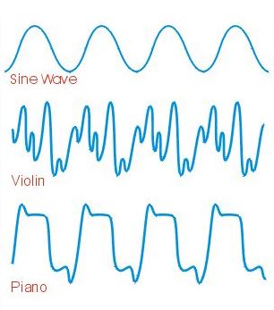
Figure 3
I will borrow some explanation of harmonics from reference 5. It explains that the instrument produces different wave shapes based on the shape of the instrument. that demonstrate comparison of wave shape and harmonics. Another factor is the way the note is played. “If you press a piano key and release it, the sound changes volume gradually over time. First, it rises quickly (or “attacks”) to its maximum volume. Next, the sound “decays” to a lower level and stays there or “sustains.” Finally, when we let go of the key, the sound “releases” and dies down to silence.”
” There are other factors too. An instrument doesn’t just produce a single sound wave at a single pitch (frequency). Even if it’s playing a steady note, it’s making many different sound waves at once: it makes one note (called a fundamental frequency or first harmonic) and lots of higher, related notes called harmonics or overtones. The frequency of each harmonic is a multiple of the fundamental frequency. So, if the fundamental frequency (also called the first harmonic) is 200Hz (which we can think of as simply 1 × 200Hz), the second harmonic is 400Hz (2 × 200Hz), the third is 600Hz (3 × 200Hz), the fourth is 800Hz (4 × 200Hz), and so on. Playing together, the harmonics make a dense, complex sound a bit like a barber’s shop choir, with low voices and high voices all singing in tune. The more harmonics there are, the richer the sound.”
Getting back to Analog and Digital, what the instrument is delivering is a continues series of complex waves that include small and smaller portions of the waves. Taking these waves and “chopping” them up into discrete segments has to average out the variation in each of the measurement size chunks of sound waves. So, no matter how fine one dissects the wave, there is averaging with each bite-sized piece of the actual music. It is possible to take that measurement down to a small enough size that the typical listener will not notice the subtle differences from the analog. BUT, sound can also be subtly felt. No matter how small the averaging size, there will be a difference from the original analog sound wave. Consequently, vinyl (records) is making a come back due to the superior reproduction of actual sounds due to vinyl being an analog delivery of the sounds.
References:
- https://www.intmath.com/trigonometric-graphs/music.php
- https://www.shaalaa.com/question-bank-solutions/two-musical-notes-of-the-same-pitch-and-same-loudness-are-played-on-two-different-instruments-their-wave-patterns-are-as-shown-in-following-figure-properties-of-sounds_36995
- https://dsp.stackexchange.com/questions/46598/mathematical-equation-for-the-sound-wave-that-a-piano-makes
- https://www.google.com/search?q=violin%20sound%20wave&tbm=isch&client=firefox-b-1-d&hl=en&sa=X&ved=0CCAQtI8BKAFqFwoTCMD74Mi9-YEDFQAAAAAdAAAAABAU&biw=1542&bih=994https://www.google.com/search?q=violin%20sound%20wave&tbm=isch&client=firefox-b-1-d&hl=en&sa=X&ved=0CCAQtI8BKAFqFwoTCMD74Mi9-YEDFQAAAAAdAAAAABAU&biw=1542&bih=994
- https://www.explainthatstuff.com/synthesizers.html