
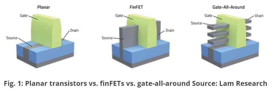
Semiconductors are always in the news as the drive for greater capabilities in ever decreasing package sizes. With the announcement of 3nm node devices going into production, the challenges continue to increase. TSMC has started a pilot production of 3nm devices [Ref. 1]. The shrinkage in size is at the point where there are needs for new transistor designs. The direction appears to be moving from FinFET to a Gate-All-Around FETs design. Figure 1 is from reference 2.
Obviously, there are manufacturing challenges. One of the proposed GAA FET designs is based on nanosheets of material. It appears that some manufactures will introduce the nanosheet FET at 3nm and others at 2nm. (More details on the development of the FETs can be found in reference 2.)
Research at Tsinghua University in Beijing, China have developed a transistor with atomically thinned channels that have a gate length of 0.34nm. [Ref. 3 & 4] This is still years from manufacturing possibilities if it happens at all. Multiple technologies are developed, but a very limited number are able to be developed where the process would work in volume manufacturing. However, this work indicates there a possibilities for continued reduction in the size of the transistors.
Researchers at Georgia Tech, Tianjin University, and Kwansei Gakuin University have demonstrated a nanoelectronics platform based on graphene [Ref. 5]. The process employs e-beam lithography to connect the edges to silicon carbide devices. If oxygen can connect to the graphene, it becomes graphane, which is an insulator.
There are other options for improving the performance capabilities of the semiconductor devices. Chiplets [Ref. 6] are small elements of a circuit that can be employed across a large variety of devices. The advantages of chiplets include the ability of co-locating processors with memory immediately adjacent. This reduces the time it takes a signal to move to or from memory, which results in improved performance. But, nothing is without challenges. Reference 7 covers the need for heterogeneous integration to create multi-die packages. The advantage of smaller area die/chips provides the ability to increase yields due to less complex individual semiconductor functions.
There is another consideration when stacking chiplets. A single semiconductor die is built into a package that dissipates heat to keep the device temperature from becoming too hot. Stacking one or more chiplets removes these portions of the circuitry away from a heat sync. The buildup of heat will impact performance and could have an adverse impact on long-term device reliability.
All of the efforts within the semiconductor industry and researchers worldwide has coordination. In the 1990s, the International Technology Roadmap for Semiconductors (ITRS) was developed to provide guidance for researchers to address future needs that would be required to be in production over the next 10 to 15 years. This roadmap was updated annually. The roadmap committee restructured the ITRS format to address seven different technology areas. The roadmap was renamed the International Roadmap for Devices and Systems (IRDS) to more appropriately address the needs of the complete process. The responsibility of the IRDS was moved from the roadmap committee to the Institute of Electrical and Electronic Engineers (IEEE). The focus of the IRDS is still the requirements for the next fifteen years on a continually moving basis. More details and the roadmap are available is reference 8.
Changes are coming to semiconductor technology that will improve the performance of devices and create new opportunities for innovate products that require greater computing power.
References:
- https://auto.economictimes.indiatimes.com/news/auto-components/tsmc-begins-pilot-production-of-3nm-chips/88071568
- https://semiengineering.com/new-transistor-structures-at-3nm-2nm/
- https://www.tomshardware.com/news/semi-transistors-atom-thick
- https://www.nature.com/articles/s41586-021-04323-3
- https://www.graphene-info.com/researchers-take-step-towards-graphene-electronics
- November 2022 Blog http://www.nano-blog.com/?m=202211
- https://semiengineering.com/heterogeneous-integration-co-design-wont-be-easy/
- https://irds.ieee.org