
Last month’s blog covered changes that are coming in the structure of semiconductor transistors. With the announcement of 3nm devices [Ref. 1}, there is no uncertainty that the structures are being designed in the small nanoscale region. As this shrinkage continues, the application of 2 dimensional materials (2-D) is increasingly important.
Energy efficiency of devices is important in order to continue miniaturization of devices and provide improved performance. A devices, like phones, add more functions in roughly the same form shape and size, the ability to have longer battery life (more power for a longer time) is more important. This same ability is key for creating electric vehicles (EVs) with increased travel range. Solutions are developed, but the process sometimes can take a long time.
A paper [Ref. 2] in 2015 describes work started in 2011 on improved layering methods to produce 2-D materials with interesting properties. Work has been focused on transition metal dicho9cogenides. This examines the properties of the combination of one of the 15 transition metals (Molybdenum, Tungsten, etc.) with one of the chalcogen family (sulfur, selenium, and tellurium). At that time, there were hopes to develop a combination that could be employed in place of silicon. The work in 2015 expanded the original possibilities by sandwiching a transition metal, like titanium, between monoatomic layers of another metal and employ carbon atoms to bind the layers together and produce a stable material. The key to their success is the discovery of a material called MAX phase. (M is for the transition Metal, A is for “A group” metals, and the X is for carbon and/or nitrogen.) This terminology was based on material developed in 2011 and called “MXene”, which is based on the process of etching and exfoliating atomically thin layers of aluminum from MAX phases.
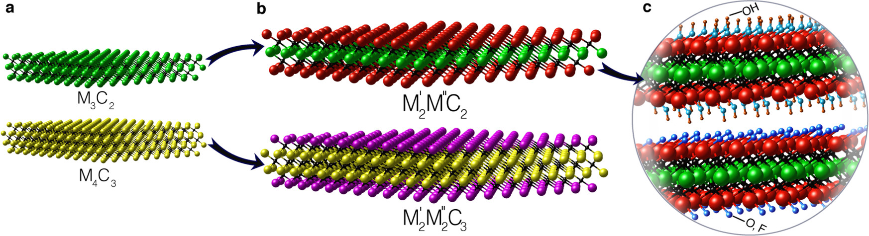
Figure 1 is from the authors paper [Ref. 3] showing the detailed structure of the MXenes.
“Schematics of the new MXene structures. (a) Currently available MXenes, where M can be Ti, V, Nb, Ta, forming either monatomic M layers or intermixing between two different M elements to make solid solutions. (b) Discovering the new families of double transition metals MXenes, with two structures as M′2M″C2 and M′2M″2C3, adds more than 20 new MXene carbides, in which the surface M′ atoms can be different from the inner M″ atoms. M′ and M″ atoms can be Ti, V, Nb, Ta, Cr, Mo. (c) Each MXene can have at least three different surface termination groups (OH, O, and F), adding to the variety of the newly discovered MXenes”. [Ref. 3]
Fast forward to 2023, a report [Ref. 4] describes the anticipated advantages of the MXenes in a number of potential applications. MXenes are produced as nanometer thick flakes, which can be dispersed in water or other solution and applied to surfaces. Work has been done to create a supercapacitor and apply it to fabric. The material has been demonstrated to be able to power a 6-volt device for over an hour. While this seems promising as a replacement of lithium-ion batteries, there are issues. The MXenes tend to oxide and degrade in normal conditions. A solution has been demonstrated employing high frequency acoustic waves to remove the rust. It is a fast process that is repeatable. The contention is that the MXenes created for this purpose have four times the storage density of Lithium-ion batteries.
Additional work on employing MXenes, with characteristics favorable to sensors, for medical purposes, such as detecting cancer. Combining the MXenes with a gold nanoarray provided a base for in -situ testing. Adding specific biosensors for identifying specific biomarkers has been demonstrated. This is an early effort to improve detection of specific cancers. There is much research still required to develop this as a usable device.
While there has been a number of promising applications, the immediate availability is not happening. One of the reasons is that there is no source for a consistent supply of the material. The challenge will be to develop processes that provide consistent high-grade material. Until then, MXenes are a great material for developing materials that could have breakthrough results.
References:
- https://auto.economictimes.indiatimes.com/news/auto-components/tsmc-begins-pilot-production-of-3nm-chips/88071568
- https://spectrum.ieee.org/why-mxenese-matter
- https://pubs.acs.org/doi/full/10.1021/acsnano.5b03591
- https://spectrum.ieee.org/new-method-for-layering-2d-materials-offers-breakthrough-in-energy-storage