Energy from Fusion – As reported in Phys.Org [Ref. 1] a breakthrough announcement in fusion came from Lawrence Livermore National Labs. For the first time an experiment in fusion created more energy that was required to generate the fusion. Unlike nuclear reactors which employ radioactive materials to generate power, fusion does not have radioactive materials involved. The process is often described a how the sun creates its energy. The idea behind the decades of research is that fusion energy would be clean (green) and a reliable source.
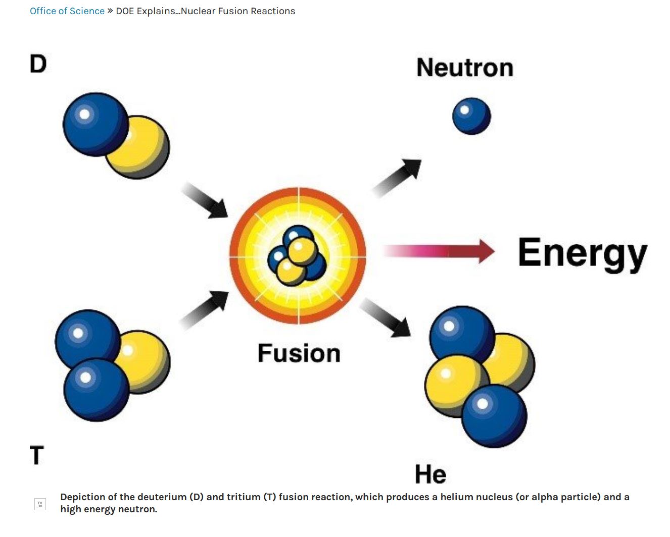
What is the fusion process? The effort on developing fusion energy employs hydrogen. (A little chemistry needed.) Hydrogen in its most abundant form consists of one proton and one electron. There are two other forms of hydrogen. Deuterium, which consists of one proton, one electron, and one neutron, and Tritium, which has two neutrons. What is necessary to create energy is to combine one atom of Deuterium with one atom of Tritium. The result of this combination is one atom of helium, one neutron, and energy [image from Ref. 2].
The challenges for this process include the fact that the temperature required is millions of degrees at pressures that force the hydrogen atoms together. Normally, hydrogen atoms would repel each other. In these conditions, hydrogen becomes a plasma and not a gas. This requires constraining the plasma, which requires a magnetic bottle. Making this happen pushes the state of current technologies. The current experimental construction employs 192 very high power lasers focusing on a very tiny spot. In that tiny spot is a small pellet containing the two different isotopes of hydrogen. The entire container is roughly 2,000 microns. There has been some information that the successful test used a modified shell thickness. There is a reasonable probability that the modifications in the thickness were in the nanometer range.
This effort was a proof of concept. It is estimated that the energy produced for a fraction of a second was greater than all the power generation in the world for that same time. This is only the next step in the development of fusion power. But, it is a significant step proving that power can be generated. Not everyone agrees with fusion power. Reference 3 has opposing opinions.
Graphene highlights – Graphene has dropped from view as it becomes more integrated into everyday products. However, there are developments occurring. Researchers at the National Graphene Institute employed graphene as an electrode to measure electrical force applied to water and the resultant rate of separation [Ref. 4]. Developing these parameters should permit the improvement in being able to extract hydrogen from water. Hydrogen for a fuel is being explored by a number of companies.
Researchers at Northeastern University (Boston) and University of Texas at Arlington have developed a process to measure the topmost atomic layer of materials. [Ref. 5] They have identified the process as an auger-mediated positron sticking (AMPS). A key element is that when positrons change from vacuum state to surface bound, the state change excites electrons into the vacuum. More detail is available in the reference.
A nano-based electronics platform has been developed by researchers at Georgia Tech, Tianjin University, and Kwansei Gakuin University. [Ref. 6] The premise is that this graphene-based platform is compatible with conventional, silicon semiconductor technology. The thought is that using this new platform for electronics will produce smaller and stronger circuity.
Scientific Integrity – Unfortunately, this is a topic that has been covered multiple times over the last few years. Some times research results have erroneous conclusions, incomplete data, or “fitting” data attempting to prove a hypothesis. The most recent report, published December 15, 2022, [Ref. 7] that has raised controversy is from the Agency for Healthcare Research and Quality, which is part of the US Department of Health and Human Services. Their work estimates there are 130 million emergency department visits per year within the United States. Using an average of 25,000 visits per department results in approximately 5,200 emergency departments in the United States. Their report indicates there are 50 deaths per facility per year or 260,000 deaths per year in emergency departments due to diagnostic errors! These conclusions were republished in late December 2022 by the DC Medical Malpractice & Patient Safety Blog [Ref. 8], on Twitter [Ref. 39 by the New York Times, and in the UK Daily Mail [Ref. 10]. This information is spreading world-wide.
There is a problem with this report that relates to scientific integrity. An article published in the Wall Street Journal, December 30, 2022, [Ref. 11] raises questions about the accuracy of the report conclusions. That article points out that the implication that one out of every 500 patients die of physician error. It questions the statistical method employed. The total number of patients in the study was 503 with one patient dying due to a delayed diagnosis by an ER physician. This article also points out that the study was focused on all kinds of medical errors and not specifically to estimate death rates from erroneous or late diagnoses. The sample size was insufficient to allow that type of a conclusion.
The result is that a report with shocking results, ¼ million emergency room deaths due to physician error, raises questions about the medical profession. When errors in the process demonstrates that the conclusions are inaccurate, it raises questions about the researchers and their organizations. As a side issue, the study was made in Canada using Canadian emergency room data. How does this demonstrate what happens in the United States? There have not been any clarifications issued as of the date of this blog. When issued, any clarification can not undo the damage of the published data in various media.
References:
- https://phys.org/news/2022-12-nuclear-fusion-scientists-latest-breakthrough.html
- https://www.energy.gov/science/doe-explainsnuclear-fusion-reactions
- https://www.counterpunch.org/2022/12/28/nuclear-fusion-dont-believe-the-hype/
- https://statnano.com/world-news/96864/Researchers-use-graphene-to-measure-the-properties-of-a-material%E2%80%99s-surface-layer
- https://www.graphene-info.com/researchers-use-graphene-electrodes-split-water-molecules
- https://www.graphene-info.com/researchers-use-graphene-electrodes-split-water-molecules
- Diagnostic Errors in the Emergency Department: A Systematic Review https://effectivehealthcare.ahrq.gov/products/diagnostic-errors-emergency/research
- https://www.jdsupra.com/legalnews/misdiagnoses-lead-to-250-000-er-8669286/
- https://twitter.com/nytimes/status/1604012290734522368
- https://www.dailymail.co.uk/health/article-11546585/ER-misdiagnoses-kill-quarter-million-Americans-year.html
- https://www.wsj.com/articles/false-alarm-about-emergency-rooms-ahrq-physicians-er-misdiagnoses-mortality-rate-us-canada-trust-11672136943