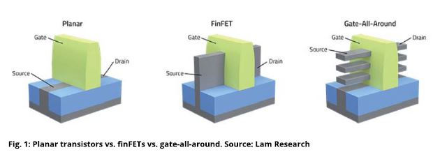
Interesting Times due to Interesting Discoveries

In previous blogs, two dimensional semiconductors have been discussed.  Work at Singapore University of Technology and Design has developed a different approach to solving the issues of very small transistors that will be required for future generations of semiconductors [Ref. 1].  Their work demonstrated that the 2D semiconductors using MoSi2N4 and WSi2N4 form Ohmic contacts with titanium, scandium and nickel.  These structures are free from Fermi Level Pinning (FLP), which is present in other 2D semiconductors.  Their approach to minimize the FLP requires a precise positioning of the metal on top of the semiconductor, which employs the 2D metal as contact material.  Their material is shielded due to the formation of an inert Si-N layer shielding the semiconductor layer from defects and material interactions at the contact interface.  They are planning to employ computer evaluations of similar materials to determine other potential materials.

Work is continuing to find improved material for Chemical energy, which could provide storage via chemical energy that can be converted into mechanical energy.  Chemical energy is a term for the energy stored in covalent bonds holding atoms together in molecules.  Work accomplished at the University of Buffalo, University of Maryland and Army Research Labs evaluated the potential of combining energic materials with ferroelectrics to create a high power density energy source that would be chemically driven.  The reported results are that two dissimilar materials (molecular energetic materials and ferroelectrics) can be combined to obtain chemically created electrical energy with a specific power of 1.8kW/kg.  Employing a polarization of molecular energetic ferroelectrics can provide control of both the energy density and the rate of energy release.

Work at Northwestern University and Argonne National Labs has developed a material that is four atoms thick and allows the evaluation of charged particle motion in only two dimensions [Ref. 3].   The target material was a combination of silver, potassium, and selenium.  Heating this material to over 450F, it became a relatively symmetrical layered structure.  Before the heating, the silver ions were fixed within the two dimensional material.  After the transition due to heating, the silver atoms had small movement.  This discovery has the potential to provide a platform for the evaluation of materials that could be constructed to have both high ionic conductivity and low thermal conductivity.  One of the potential outcomes is the ability to develop membranes that could provide environmental clean including desalting of water. 

A team of researchers at the University of Florida and Florida Institute of Technology have produced a high-efficiency mechanical signal amplification in nanoscale resonators operating at radio frequencies [Ref. 4].  The researchers observed parametric amplification in nanoscale devices.  The device contains a nanoscale drumhead mechanical amplifier consisted of a two dimensions semiconducting  molybdenum disulfide membrane with drum head thickness of 0.7, 2.8, and 7.7 nanometers.  The drum head was 1.8 microns in diameter with a volume of 0.020 m3.  The drum head was fabricated by transferring nanosheet exfoliated from bulk crystals over microcavities to make the thin nanodrums.  Amplification gains of up to 3600 were obtained.  This process can be employed in developing nanoscale sensors and actuators. 

What we are witnessing is the development of new materials that have been able to be developed due to the ongoing research in nanotechnology and the resultant development of tools for analysis of the various materials. 

References:

  1. https://scitechdaily.com/newly-discovered-family-of-2d-semiconductors-enables-more-energy-efficient-electronic-devices/
  2.  https://www.nanowerk.com/spotlight/spotid=58913.php
  3.   https://scitechdaily.com/unplanned-discovery-a-super-material-for-batteries-and-other-energy-conversion-devices/
  4. https://phys.org/news/2021-10-highest-amplification-tiny-nanoscale-devices.html
Misc Ramblings

Evolving nano developments

With the emphasis on nanotechnologies and the emphasis on two-dimensional materials, other areas that are pushing boundaries are often overlooked.  A recent article [Ref. 1] summarizes work done at King’s College London on relieving pain.  Their treatment employs a ultra-low frequency neuromodulation to safely relieve chronic pain.  Neuromodulation employs electrical current to block transmission of pain signals between neurons.  The procedure normally requires implanting a device and sending signals.  Spinal cord stimulation is one example of this procedure.  Unfortunately, the success of that process has been less than desired.  This new method, employs a type of ultralow frequency biphasic current with a period of 10 seconds.  The process mimics the direct current applications, which can cause tissue damage and electrode degradation.  Due to the nature of the alternating polarity there is the potential for much reduced tissue damage.  Work is continuing in the area.  For further information the Wolfson Centre for Age-Related Diseases [Ref. 2] has additional information regarding their ongoing work.

A team of Chinese researchers has developed an interesting “twist” to graphene [Ref. 3].  By placing a second layer of graphene over the first and creating a slight misalignment, they created a Moire superlattice.  As the angle approaches 108 degrees, the material begins to show properties that imply low temperature superconductivity.  The result is that the kinetic energy of the electrons is suppressed and form localized accumulations at points where the two sheets interact.  There are additional effects that include correlated insulator states.   This is important because integrated photonics require nanolasers.  (Data transmission on a chip can travel at the speed of light.)  The work to produce these nanolasers has focused on a number of approaches, but the material properties for th4ese approaches has not been developed at the nano scale required for inclusion on semiconductor devices.  The referenced paper provides specifics on the low power required for lasing.  The researchers indicate their opinion that this development has the potential to impact many fields including “nonlinear optics and cavity quantum electrodynamics at the nanoscale.” [Ref. 4]

Researchers from Rice University and Northwestern University created a stable sheet of double layered borophene [Ref. 5].  This is a material structure is similar to graphene (Carbon sheets).  The atomic number of Boron is 4.  Carbon is 6.  Research is indicating that the borophene has electrical and mechanical properties that could rival graphene.  The difference is that the borophene is much more challenging to create.  The researchers succeeded in growing the material on a metal substrate.  Boron, when attempts to create the double sheet structure, tends to revert to its three dimensional structure.  The researchers think that the borophene structure could produce a much greater type of structures than graphene.  One projection is the potential for inserting a layer of lithium to create a superior two dimensional battery. 

As always, these developments don’t happen over night.  The work on borophene has taken over 6 years.  This will be followed by experimentation to develop a reasonable means of creating the materials. Only after that is available can products be produced that will appear in the public arena.

References:

  1. https://physicsworld.com/a/ultralow-frequency-neuromodulation-safely-relieves-chronic-pain/
  2. https://www.kcl.ac.uk/neuroscience/about/departments/card
  3. https://physicsworld.com/a/moire-superlattice-makes-magic-angle-laser/
  4. https://www.nature.com/articles/s41565-021-00956-7
  5. https://physicsworld.com/a/double-layered-borophene-is-created-at-long-last/
Nanotechnology

More on Semiconductors

Last month, this blog covered some of the challenges of continually shrinking semiconductor geometries and the related difficulties with traditional transistor designs.  This month’s blog explores transistor geometry.  In May 2021, IBM announced a 2nm nanosheet semiconductor technology. [Ref. 1]  Their claim is that this configuration will improve performance while consuming only 45& the energy as the current generation of chips. 

The nanosheet technology is one where the transistors are constructed from three horizontal sheets of silicon with the gate material surrounding the silicon.    The nanosheet technology is projected to replace the existing FinFet technology, which is approaching the limits where is can function properly due to material characteristic limitations.  The transistor configuration has developed through various shape configurations, but the materials have remained the same. [Ref. 2]  The transistor employed in microprocessors consist of a gate stack, a channel region, a source electrode, and the drain electrode.  The latter three are all based on silicon but have different doping atoms (impurity atoms introduced during processing to create the desired electrical properties).  The gate stack consists of a gate electrode on a layer of dielectric material.  The dielectric material is employed to ensure that the electrons flow when appropriately charged and not subject to random leakage of electrons. 

When the size shrinkage became too small to prevent current leakage, today’s FinFET transistor was invented and introduced into production in 2011.  With current production at the 7nm node and moving to the 5nm, Samsung has stated the FinFET design has run out of capability at 3nm.  A new design needs to be developed.  The new design is the nanosheet, although there are a few other names, like GAA (gate-all-around).  The picture below (from Ref. 2) depicts the design evolution of transistors.  The nanosheet design was announced by IBM for the 2nm node (Intel is call the node the 20 Angstrom node).

The introduction of a change in design will provide a number of challenges that manufacturing needs to overcome.  Since there is similarity between the nanosheet and the Fin FET, some of the process learning can be accelerated.   There are innovations required.  [Ref. 3]  The first is the need for epitaxially grown multilayers of Si and SiGe to define the channel.    Next, the nanosheet design requires an inner spacer, which is additional dielectric material for source/drain isolation.  Third is the separation of nanosheets from each other, which requires a very selective etch process.   Finally, there is the deposition and patterning of metal around and in between the nanosheet layers.  As mentioned earlier, this design enhancement is anticipated to reduce power usage by 45%. 

What happens when nanosheet runs it course?  There are designs being considered called forksheet.  [Ref. 3]  The challenges are numerous and also include a concern about electrostatic discharge.  Also, under consideration is something called a CFET or complementary FET.  This design employs vertically stacked nMOS and pMOS. 

Consequently, changes are coming to semiconductors.  The devices will become smaller, more powerful, and use less energy.  The manufacture of the devices will push the existing limits of current manufacturing and require the invention of new techniques and new equipment.  It will be very interesting to observe the changes in devices as semiconductors move to smaller and smaller node and start reducing power required.  Good things are coming.

References:

  1. https://spectrum.ieee.org/ibm-introduces-the-worlds-first-2nm-node-chip
  2. https://spectrum.ieee.org/the-nanosheet-transistor-is-the-next-and-maybe-last-step-in-moores-law
  3. https://www.eetimes.com/entering-the-nanosheet-transistor-era/#

Semiconductor Technology

The Shrinking Dimensions

As semiconductor manufacturing continues the dimensional shrinking process, novel ideas are required to achieve the ability to continue shrinking the dimensions while increasing the performance.  There are some thoughts that this potion of the Moore’s law curve will provide some additional benefits.

As the industry moves into the sub 10 nanometer nodes, physical properties become major role players in what will be able to be manufactured in volume *with sufficient yields) and what won’t work.  Intel has released its roadmap [Ref. 1] for the smaller dimensions and is moving away from the nanometer scale.  After the 3nm node, it will not be the 2nm node. Instead, it will be the 20 Angstrom node. That will be followed by the 18 Angstrom node.  [An Angstrom is 10-9 meters or a tenth of a nanometer.  It is not a new term. Angstroms were used in optics for hundreds of years.].

While the size terminology is interesting, it is the actual physical propertied and the manufacturing of the completed devices that are the objective. 

Filed Effect Transistors [FETs], and specifically MOSFETs manage current flow by controlling current flow.  The gate electrode and the channel are two plates of a capacitor.  Unfortunately, the gate capacitance depends on the material properties at the dimensions required.  The loss of the needed parameters as size shrinks is driving the investigation to what are being called two-dimensional semiconductors. [Ref. 2] More detail on this topic is available in our April 2021 blog. [Ref. 3]

In the article with Intel’s planned roadmap, there is mention that starting at 20A, Intel is considering changing to a “gate all-around” structure [GAA].  The Intel approach is somewhat different from others working on GAA and their modification is being called the ribbonFET.  [Ref. 1]

Another topic of current interest is “chiplets”.  [Ref. 4] The concept behind this is to create individual segments for a system and be able to place them in positions that are favorable to data transfer and processing.  This approach is a means of reducing costs while achieve apparent scaling benefits.  On a larger scale there are many companies working on various approached to reduce dimensions by using multiple levels (this is not multiple layers) with interconnections to complete the system interconnections.  I know of one sensor system that has multiple levels for a complete autonomous sensor system with capabilities of working in temperatures of over 120C and over 10K PSI.  It has sensors and can store data for up to a week before being wirelessly interrogated for data transmission.  This device is under 8mm in diameter.  It will be shrunk to under 5mm in the near future but taking it to under 1,000 microns would be a challenge without moving to something like the chiplet approach.

While the topic of semiconductors is mainly about shrinking feature sizes and increasing processing capability, the real changes will come from nanomaterial characteristics.  The fact that today, researchers are developing a method to layer different 2-dimensional materials together indicates the direction.  For this to be successful, the method to develop large scale 2-D material without defects still remains a challenge.  It will happen, but will require development efforts.

References:

  1. https://www.eetimes.com/intel-charts-manufacturing-course-to-2025/#
  2. https://semiengineering.com/thinner-channels-with-2d-semiconductors/
  3. http://www.nano-blog.com/?m=202104
  4. https://semiengineering.com/piecing-together-chiplets/?cmid=291477a6-f062-4738-b59f-1ec44fd21e39
Misc Ramblings, Nanotechnology

More on Cement and other Nano

Just prior to the end of June, there were two articles on cement/concrete.  “How to Make a ‘Smarter’ Cement” [Ref. 1] covers reports from Northwestern University’s team that introduced nanoparticles into ordinary cement.  They investigated two types of nanoparticles and the impact on fracture toughness.  The material employed was graphene in both the shape of rolled tubes (carbon nanotubes) and also as flakes.  Incorporating small amounts of nanomaterial improved the bonding due to tightening the pore structure, which reduced the air voids.  It was pointed out that this structure was replicating nature.  They chose to replicate the multilevel structure with the nanoparticles and the cement.

The second article [Ref. 2] address the variety of application.  This BBC report covers the vast array of cement that is being employed around the world.  The article is interesting in the fact that it includes a vast array of structures both modern and ancient.  The Pantheon in Rome was built in the second century AD and is still the world’s largest unreinforced concrete dome.  This structure’s existence  implies that Roman Cement was superior to what we are currently using in present day construction.  (cf. last month’s blog)

There is more material in published reports on the need for 2D semiconductors.  This is especially true as the dimensional for the 3nm and 2nm semiconductor nodes are investigated.   Reference 3 is one of many such articles.  As the dimensions of the transistor decrease, there needs to be a corresponding reduction in thickness.  Control of the electron flow is critical.  Nanosheets and nanowires are being considered along with the gate-all-around transistor.  The issues arise at the 3nm scale with trapped imperfections in the materials.  2D material appears to provide a possible solution.

From my viewpoint, the issue with 2D material is the production of large quantities of defect free material.  There are various materials being investigated with transition metal dichalcogenides (MoS2, WS2, and WSe2 are most commonly proposed).  The materials of choice are flakes of material exfoliated from bulk material.  (Might bring back some memories of the early carbon nanotube work.)  Atomic Layer Deposition (ALD) can provide think layers but there are residues left behind by the process that can contaminate the desired material.  There is a lot of research being conducted, but much more needs to be accomplished before the 2D process can be ready for producing semiconductors on the scale needed.

From the medical standpoint, graphene and CNTs are being employed in developing sensors.  A team from Harvard [Ref. 4] has created a flexible electrode array that conforms to surfaces of the body.  The example application was described as being applied in difficult to reach places in order to provide recording or stimulation of electrical pulses without the potential of damaging nearby organs.  The team developed the gel and needed to create the required circuitry.  They developed a combination of graphene flakes and CNTs that could provide a continuous conductor path.  When created on the gel, the long CNTs provide a “long” continuous pathway by multiple point contact among numerous CNTs.  They then insulate it on the gel so that only the desired points are exposed.  They have successfully tested the gel in stimulation a mouse heart.  A key point in their development is that they needed to find some means of reducing the metal content required for conductivity.  And, they succeeded.

What we are witnessing is novel thinking in applying different type nanomaterials to solve problems that challenging to resolve with current technology applications.

References:

  1. https://www.techbriefs.com/component/content/article/tb/stories/blog/39416
  2. https://www.bbc.com/future/article/20210628-concrete-the-material-that-defines-our-age
  3. https://semiengineering.com/thinner-channels-with-2d-semiconductors/
  4. https://www.graphene-info.com/graphene-and-cnts-assist-creating-viscoelastic-electrode-arrays
Nanotechnology

Nanomaterials and Cement

It has been an interesting month as the country starts coming back to “normal”.  I was fortunate to have the opportunity to “attend” (virtually) a presentation by a University of Texas at Austin professor.  Professor Hugh Daigle provided a very informative presentation on “Nanotechnology for Upstream Oil and Gas Operations”. [Ref. 1]  Whether you are interested in Oil and Gas or not, there are some very interesting points that are important where your nanotechnology interests are.  The reference is to a YouTube video of the presentation. 

The presentation starts out with establishing the baseline of what is nanomaterial.  The slide at roughly 7:35 of the presentation presents why nanoparticles are so interesting.  This is followed by covering the forces that are important to consider at the small scale.  Most are aware of Electrostatic and van der Waals forces.  The Steric forces are not mentioned as much as the two previous ones.  The description of the application is interesting and has a good explanation of applications. 

Jumping forward to roughly 22:24 in the presentation the explanation of controlling nanoparticle surface charges is important to improving the properties of cement.  At roughly 25:30, he goes into an explanation of why this sizing of the nanoparticles can improve the properties of the cement.

Daigle’s presentation fits into an special area of my interest.  We know that the Roman Coliseum is still standing after 2,000 years.  We can not duplicate their efforts.  Research has been done and there are some interesting findings.  Reference 2 has the explanation that has been acccepted without too much understanding.  Basically, the Roman cement was superior due to using volcanic ash from the regions around the Gulf of Naples.  Also, it is known that the Roman cement cures under water, salt water to be precise.

The work reported in Nature by Alexandra Witze [Ref. 3] has taken this a step further.  A team headed by Marie Jackson discovered there is a very rare mineral formed in the Roman cement. [Ref. 4]  This mineral, aluminum tobermorite comes from a silicate mineral, phillipsite, which is common in volcanic rocks.  Their finding also identified crystals of aluminum tobermorite growing from it.  Apparently the tobermorite is grown from phillipsite by the action of salt water washing through the cement.  This increases the alkalinity of the cement.  It is a rare material.  The tobermorite strengthens the cement due to a plate-like structure that permits flexure not observed in today version of cement. 

Now, I come back to Professor Daigle’s presentation.  He talked about the size of the nanoparticle has a significant influence of the strength of the cement. To me the question I have is did the Romans develop a process that created a consistent size of nanoparticle that yielded the optimum size for the most strong cement?

For the doubters that think the Romans would not have sufficient knowledge/understanding to know that they needed a certain size material (nanoparticle), consider this fact.  In the Middle Ages, the artisans knew they needed a certain size gold nanoparticle to create the red coloring in stain glass windows.  Did they call it gold nanoparticles?  Of course not, but there had to be a process, probably milling, that after a certain time of processing yielded the proper size material to create the red color.  It is possible that the Romans could have had a similar process for the phillipsite.

It does provide some interesting questions about the capability of the Romans and their cement. 

References:

  1. https://youtu.be/cWzzR5h535g
  2. https://newscenter.lbl.gov/2013/06/04/roman-concrete/
  3. https://www.nature.com/news/seawater-is-the-secret-to-long-lasting-roman-concrete-1.22231
  4. https://www.degruyter.com/document/doi/10.2138/am-2017-5993CCBY/html
Nanotechnology

2D Materials are Making Progress

The recent past few months have seen a few published articles on 2D materials and their applications.  The pace is picking up.

One of the challenges of 2D materials is that the materials need to be incorporated into some other material.  A future possibility for semiconductor device transistors requires there must be a means of combining the 2D material with the silicon (or other material) substrate rapidly and in volume.   There are two significant issue with this combination.  One of the issues is that the 2D material and the semiconductor substrate require different temperatures that can damage the material already on the substrate.  The other is that the existing processes are not compatible with high-volume manufacturing.  Researchers in Sweden and Germany [Ref. 1] have developed a process that uses a standard dielectric and available wafer bonding equipment. 

The researchers attached the 2D material, which in on a wafer, and the semiconductor wafer.  Using pressure at room temperature, the two wafers are pressed together, and the temperature raised until the dielectric becomes viscous and allows the 2D material to conform to the surface of the existing material on the semiconductor wafer.  There efforts have been successfully demonstrated on a 100mm silicon wafer with uniform coverage and little strain in the 2D structures.

The development of 2D transistors has also been improving [Ref. 2], Professor Saptarschi Das of Penn State has worked on the viability of transistors from 2D materials.  The purpose of the research is to determine if the 2D transistor can be the future of semiconductors with a significantly reduced footprint.  This also implies the potential for faster speeds.  Reference 3 addresses the promises and prospects of 2D transistors.  It points out that there have been many proof-of-concept demonstrations.  There might be a need to evaluate the 2D transistors to a slightly different criteria to determine the performance of the devices.  This concept of transistor evaluation is also addressed in an Applied Physics Letters [Ref. 4], and it addresses specific parameters that need to be considered. 

Imec researchers are of the opinion that transistors made from 2D materials could become available in the near future [Ref. 5].  While they indicate that silicon will remain the primary source for the microscale electronics, transistors constructed from transition metal dichalcogenides have potential.  The challenge is creating a single atom layer that is a natural semiconductor. 

The need for the change in the transistor construction is due to the every shrinking geometry of the current transistor.  As the structure of the transistor becomes smaller and smaller, the potential for unwanted/spurious leakage of electrons continues to increase.  This is caused by the physical limits of the material property.  There have been design changes in the structure of the transistors, but the limits of material properties and the designs needed to circumvent this issue are continually getting more difficult.    A detailed discussion of the challenges of 2D materials and their application to transistor is available in Reference 6

The challenges of developing the most suitable material, creating an electronic structure that is efficient and fast, along with engineering a manufacturing process that is both high-speed and high-yield is non-trivial.  2D material transistors are coming, but it will take some time before 2D transistors are in main-stream production.  But, the 2D materials are coming.

References:

  1. https://www.techbriefs.com/component/content/article/tb/insiders/electronics-sensors/stories/38954?
  2. https://www.techbriefs.com/component/content/article/tb/insiders/electronics-sensors/stories/38953?
  3. https://www.nature.com/articles/s41586-021-03339-z
  4. https://aip.scitation.org/doi/10.1063/5.0029712
  5. https://spectrum.ieee.org/semiconductors/materials/coming-soon-to-a-processor-near-you-atomthick-transistors
  6. https://pubs.rsc.org/en/content/articlelanding/2015/nr/c5nr01052g#!divAbstract
Nanotechnology, Semiconductor Technology

What is the Cost of Ownership?

Recently, the term “Cost of Ownership” has been appearing in various papers about a number of topics, including wind power and electric vehicles among others.  The Wall Street Journal had an article comparing the emissions cost of a gasoline car and an electric one [Ref. 1].  But, what does the Cost of Ownership or COO really mean.

In the late 1970s and the early 1980s, the basic concept of COO was developed to provide a comparison of the generation of electricity by coal versus by nuclear.  As witnessed today in China, coal fired generation plants can be constructed for a few millions of dollars in a short period of a year or less.  Nuclear, on the other hand, takes a significant investment of multiple billions of dollars and a planning and construction process that lasts many years.  If only construction costs are considered, the coal fired approach is much better.  (Environmental impact was not as strongly considered as it is today.)

This concept – COO – was further developed by the semiconductor industry in the 1980s to justify the change from a “silk-screening” type of creating the small patterns for the circuitry to a projection of light through a mask to create the same patterns.  Each wafer (the material used on which the circuits are created) contained multiple individual complete circuits that are separated into individual devices.  The screening process involved tools that cost $10,000 to $20,000.  The optical projection tools were in excess of $100,000.  There was a throughput advantage of the optical system but not by the factor of 5 or more differential in initial price. 

An evaluation of the actual cost of the two different processes was developed.  The process for creating the actual circuitry involves multiple steps of imaging and processing to develop the layers of material that create the circuit functionality.  A difference in yield can be quantified and that is part of the cost of ownership.  The costs include the lifetime of the equipment, the materials actually consumed, operating costs, and the actual yield of the product produced.

As an example, assume the optical method produced one more good wafer equivalent per hour and each wafer was worth $1,000 with each good device worth $50.  (The optical process created more good devices on an equivalent number of wafers compared to the screening process.) If the system ran only 240 hours per month, the extra value of the optical process would be $240,000 per month!  That makes the $100,000 cost of the optical tool was not an issue.  Consequently, the semiconductor industry changed its process. 

In the 1990s and 2000s, there was further refinement in the semiconductor industry to incorporate more variables including repair costs and the resultant value of the loss of product.  This COO process is moving to a total life cycle cost of ownership evaluation.  As the approach is applied to new industries, the inclusion of the initial costs to create the tool/process and the dismantling impact at the end of life for the equipment.  This end-of-life costs are being raised by various people regarding the batteries in general.  The standard lead-acid battery carries a replacement charge when a new battery is installed.  This is to cover the cost of separating out the component materials.  Since there is a finite life of all batteries, one would assume that the batteries projected for storing electricity during non-peak hours will have to be replaced also.

It is not unreasonable to see further developments in costing analysis to start to include the impact of the elimination of various technology products.   This might include the cost of jobs lost.  It would be difficult due to the non-measurable cost of a job and whether it could be replaced by a different set of skills.  COO is a good tool for evaluating alternatives but needs to be applied consistently and with assumptions that can be measured.

References:

  1. https://www.wsj.com/graphics/are-electric-cars-really-better-for-the-environment/
Technology

It’s time to revisit Nano Technology Safety (Nano-Safety)

Fifteen years ago (2006) there was a white paper published [Ref. 1] that addressed the need to create a structured approach to the handling and usage of nanomaterials.  As stated in the September 2013 blog on Nano-Safety, the primary issues involving nanotechnology is the concern for working with various materials whose properties are different and unknown from the bulk material.

“What is safety with respect to nanotechnology?  In the simplest terms, it is the development, manufacture, application, and control of nanomaterials in a manner that minimizes potential issues, both known and unknown that may impact both people and the environment.  All chemicals can kill one, it is just a matter of quantity.  Dangerous materials, even poisons, can be beneficial if applied in the proper dosage.  Just because something is dangerous does not mean it should not be used.  Fire is dangerous if mishandled, but does that mean we should not use it?

“One concern about safety in handling nanomaterials is based on the unknown issues.  Not knowing the impact on people or the environment can lead to unfounded concerns and a reluctance to accept developments.  This is not only true for nanomaterials but many commonly employed materials/processes when they were first introduced.  If you want to examine issues that have long had proponents and opponents, examine the application of milk pasteurization or the case of adding fluoride to drinking water.  

“In approaching this problem, … the issue of Nano-Safety can be addressed a systematic manner that involves 4 key concepts or pillars, which are: 1) Nanomaterial properties; 2) Impact on people and the environment; 3) Handling of nanomaterials; and, 4) Business focus.” [Ref. 2] 

The application of nanotechnology to health issues has seen significant developments along with related issues.  Gold nanoparticles have been employed to attach to cancer cells and then be irradiated by IR wavelength that pass harmlessly through skin but heat the gold and destroy the cancer cell that the particle is attached to.  Concerns can arise about the accumulation of the gold in the body.    

Fortunately, the tools available for investigation of the nanomaterials has been improving along with a better understanding of the interaction of nanomaterials with the human body.  

Research is approaching an interesting time.  Work is being done on nanosensors that can be connected to create a sense of “feeling” in prosthetics.  Graphene, of which research has been conducted, is now finding applications is material composite, where each layer is a single atom thick.  We are not close to large scale manufacturing – yet, but applications are being developed that promise to be able to reproduce some concepts of human feeling capabilities.  There is some work being done that could mitigate eye damage like Macular Degeneration. 

One issue that needs to be addressed is the impact of the new composites on people and the environment.  The process for long term evaluation and governmental approval is long.  This is especially true when considered to the half-life of startup companies. 

There is a need for a reevaluation of the existing guidelines for Nano-Safety and to create an update that is directed at nanotechnology and the medical environment.  The ability to expedite the development and application of nanotechnology in medical situation could provide a benefit for many.  This could be a 5th element of Nano-Safety.  More on this topic will be in future blogs.

References:

  1. Available at http://www.tryb.org/a_white_paper_on_nano-safety.pdf
  2. September 2013 blog http://www.nano-blog.com/?m=201309
Nanotechnology Safety

Let’s start 2021 out with a question.

In today’s technical reports, there are more references to Artificial Intelligence performing analyses of materials for developing an understanding of the properties of various combinations of materials at the nano-level structure.  Single layer materials are being combined with other single layer materials to produce various changes in the material properties that are not observed in the bulk realm.  As computer programs increase in complexity and capability, more and more materials are being evaluated for “interesting” characteristics. 

First consider the computers and the programs.  Prior to the mid-1980s, computers were large and relative slow.  Memory was expensive.  Expert Systems that were developed could not access large quantities of information, so the systems needed to have a table to reference its data.  The systems I built in the early 1980s used a matrix, like today’s spreadsheets, to reference probabilities of occurrences.  The system was designed to guide the worker in more quickly identifying the source of an issue.  After that specific source was identified, the worker entered the data, and the system updated the probabilities of occurrences.  An interesting observation was that employing this particular system at two different and not linked facilities provided different probabilities of occurrences at the different locations.  [References 1 & 2 are background on Expert Systems and Artificial Intelligence.  Wikipedia is also a good starting point.) 

It must be noted that there was a specialized computer developed based on MIT Artificial Intelligence that was identified as a LISP machine and had 36-bit operating system.  Interesting story [Ref. 3]

Today’s Artificial Intelligence programs have the ability to draw on a much larger database, can self-extract information from published materials, and can be programmed to continually run evaluations based on directed changes in the events/materials being selected.  While the field has grown in the Twenty-first century, there are some questions arising about the inability to prevent biases from being incorporated into the programming.  (Possibly something like the situation described about expert systems?) 

A saying that has been around for almost as long as computers is GIGO.  Garbage In, Garbage out!  The quality of the data is critical to the resultant output.  This takes us back to the application of Artificial Intelligence to evaluating novel materials.  The quality of the calculated material properties will be only as good as the data that the calculations are based upon.  There is no question that the working materials can be characterized fairly exactly.  The question is: “Do we know the material properties of absolutely pure materials?

Semiconductors are created by introducing a very small number of impurity atoms to change the characteristics of the base material.  The mathematics and the experimentation that provided the data is proven.  It works on the bulk scale.  But, what happens as the total amount of material under modification becomes smaller and smaller.  This is a serious question that needs to be answered.

In working with materials, the purity is specified.  99.99% pure is quite pure.  Six 9s is even better.  That is one part impurity in one million.  If one uses an approximation that there are 7 atoms of gold in one cubic nanometer, then there are 7 million gold atoms in a 100nm cubed sample, which implies 7 atoms that are not gold.  How does that change the properties of the material?  How do we purify gold or any other material to remove every extraneous atom?  Do we know the material properties of absolutely pure material?

References:

  1. https://azati.ai/the-return-of-expert-systems/
  2. https://www.parascript.com/blog/machine-learning-ai-vs-expert-systems-ai/
  3. https://en.wikipedia.org/wiki/Artificial_intelligence
Misc Ramblings