Last month, this blog covered some of the challenges of continually shrinking semiconductor geometries and the related difficulties with traditional transistor designs. This month’s blog explores transistor geometry. In May 2021, IBM announced a 2nm nanosheet semiconductor technology. [Ref. 1] Their claim is that this configuration will improve performance while consuming only 45& the energy as the current generation of chips.
The nanosheet technology is one where the transistors are constructed from three horizontal sheets of silicon with the gate material surrounding the silicon. The nanosheet technology is projected to replace the existing FinFet technology, which is approaching the limits where is can function properly due to material characteristic limitations. The transistor configuration has developed through various shape configurations, but the materials have remained the same. [Ref. 2] The transistor employed in microprocessors consist of a gate stack, a channel region, a source electrode, and the drain electrode. The latter three are all based on silicon but have different doping atoms (impurity atoms introduced during processing to create the desired electrical properties). The gate stack consists of a gate electrode on a layer of dielectric material. The dielectric material is employed to ensure that the electrons flow when appropriately charged and not subject to random leakage of electrons.
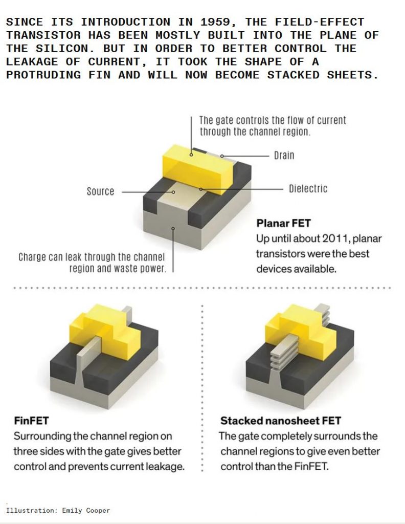
When the size shrinkage became too small to prevent current leakage, today’s FinFET transistor was invented and introduced into production in 2011. With current production at the 7nm node and moving to the 5nm, Samsung has stated the FinFET design has run out of capability at 3nm. A new design needs to be developed. The new design is the nanosheet, although there are a few other names, like GAA (gate-all-around). The picture below (from Ref. 2) depicts the design evolution of transistors. The nanosheet design was announced by IBM for the 2nm node (Intel is call the node the 20 Angstrom node).

The introduction of a change in design will provide a number of challenges that manufacturing needs to overcome. Since there is similarity between the nanosheet and the Fin FET, some of the process learning can be accelerated. There are innovations required. [Ref. 3] The first is the need for epitaxially grown multilayers of Si and SiGe to define the channel. Next, the nanosheet design requires an inner spacer, which is additional dielectric material for source/drain isolation. Third is the separation of nanosheets from each other, which requires a very selective etch process. Finally, there is the deposition and patterning of metal around and in between the nanosheet layers. As mentioned earlier, this design enhancement is anticipated to reduce power usage by 45%.
What happens when nanosheet runs it course? There are designs being considered called forksheet. [Ref. 3] The challenges are numerous and also include a concern about electrostatic discharge. Also, under consideration is something called a CFET or complementary FET. This design employs vertically stacked nMOS and pMOS.
Consequently, changes are coming to semiconductors. The devices will become smaller, more powerful, and use less energy. The manufacture of the devices will push the existing limits of current manufacturing and require the invention of new techniques and new equipment. It will be very interesting to observe the changes in devices as semiconductors move to smaller and smaller node and start reducing power required. Good things are coming.
References:
