
The common definition of “nano” is when one dimension of a material is less than 100 nm. The definition from a Google search [1] on “What is nanotechnology?” yields the following: “the branch of technology that deals with dimensions and tolerances of less than 100 nanometers, esp. the manipulation of individual atoms and molecules”. Wikipedia references [2] the National Nanotechnology Initiative’s definition, which includes: “…which defines nanotechnology as the manipulation of matter with at least one dimension sized from 1 to 100 nanometers.“ Since governmental regulations are based on this definition, let’s consider if this is a realistic method of defining nanomaterials. There is a wealth of material to consider, but only the following properties will be considered in this blog: surface adhesion, color, melting point, conductivity, reactivity, and magnetic moments.
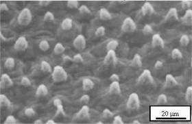
SURFACE ADHESION: There are a number of different ways to consider surface adhesion. The nano realm does not behave in ways we normally experience. The semiconductor industry requires extreme cleanliness. The issue of adhesion came to the forefront when the removal of 50 nm particles from imaging masks was an absolute necessity. The evaluation of the particle removal indicated that particles below 70 nm or 80 nm would adhere more strongly to surfaces. When the size of the material drops below 80 nm, van der Waals forces become the dominant mechanism for particle adhesion. Work in other areas have provided the ability to make glass that is self-cleaning by minimizing the ability of particles to the surface. Contrary to the perception that the flatter the surface, the harder it will be for particles to adhere is not a truism. The picture below shows a lotus leaf structure [3] which is the basis of the design of self-cleaning surfaces. By creating a surface that does not present a flat surface for materials to adhere to, the contaminate is naturally rejected.
COLOR: As mentioned in a previous blog (August 30th, 2013), the application of nanomaterials has been employed for millennia. Nanoparticles of gold have been used to give glass a red color. The picture below is from a Smithsonian article [4] and references the pictures as being supplied by the British museum. The goblet appears to be green colored until light illuminates it from the rear. It then shows its reddish color. The effect is caused by particles about 50 nm imbedded in the glass.

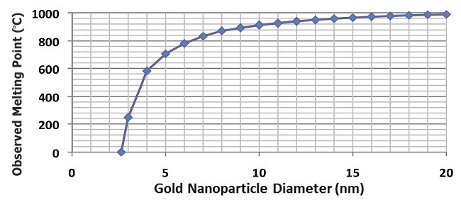
MELTING POINT: Over the centuries, one constant that people learned is that materials have a constant melting point. Gold melts at 1064.18oC, which has been determined experimentally. In fact, the various melting points for different materials can be employed to remove impurities and obtain more pure amounts of the specific material desired. Recently, the ability exists to examine the behavior of smaller sized particles. What has been found is that below 50 nm the melting point of materials begins to diminish. The curve below [5] shows the decrease of the melting point of gold as the size is diminished. [A starting point for additional information on this effect is available in reference 6.]
CONDUCTIVITY: In many respects, the conductivity issues is similar to the melting point issue. Conductivity is a bulk material property that is perceived as being a constant. Except that we are now able to work with very small material. Copper, a material valued for is conductivity, starts to have potential issues as the width of the conductors shrink below 50 nm. Effects of grain boundaries and crystal orientation can cause two similar sized conductors to have different conductivity. Consequently, precautions are required in semiconductor manufacturing processes to minimize the potential variance among conductors.
REACTIVTY: The increase of surface area provides for an increase in reactivity. This is one of my favorite points when someone wants to include all material under 100 nm as being nano and should be considered the same regardless of the size. Consider a jar of 80 nm aluminum particles. How carefully should it be handled? There is the obvious concern about opening it and having some of the dust inhaled or possible attached to one clothing. It is advisable to be cautious, but there is nothing obviously dangerous about the container and its contents as long s proper handling is observed.
According to the desire to create one classification of all 100 nm or smaller similar material, in this case aluminum, it makes no difference as regard to the size of the material. Consider a jar of 30 nm aluminum. Obviously, the same precautions need to be taken as the 80 nm material. BUT, and this is a key difference, 30 nm aluminum particles react when exposed to air (oxygen). Chemists classify the reaction as being very energetic. To the lay person, it is an explosion! Yet some regulation agencies want to classify both sizes as being identical. Really? There is some effort in France to include exposed surface area in the classification of nanomaterial.
MAGNETIC MOMENTS: There are a limited number of materials that are considered to have magnetic properties. The nano realm always provides surprises. “There are a number of materials that are known to have magnetic properties, and they do not include either silver or platinum. However, 13 atoms of silver have been shown theoretically to have a magnetic moment, and 13 atoms of platinum has been shown experimentally to have a magnetic moment. [8 & 9] This is a new property for these metals.”[7]
THOUGHTS: Establishing a standard or regulation based on a simple property as 100 nm or less does not guarantee that the issued document appropriately addresses the concerns. Material Safety Data Sheets (MSDS) become questionable at best. A nano-MSDS that is 17 pages long will not be effective, nor are there enough resources to produce an MSDS for each 1 nm variation of particle size.. The effort of DuPont and the Environmental Defense Fund to develop the Risk Framework is an excellent starting point. But, how does one really know what the material properties are. If there are a distribution of particles, and there are always some size differences, how does one quantify the material properties? Our experience is that we can go to a table and find a property, but at the nano scale the properties are changing with size. Does a distribution of 10 nm gold particles (0.5 nm half-width) have the same properties as a similarly sized distribution with a half-width of 3 nm? Will they melt the same way? What happens when one looks at the impact of multiple effects on the nanoparticles? Currently, bulk material properties have two-dimensional curves for the properties, e.g., the boiling point of water is a function of temperature and pressure. Does this imply that the proper description of nanoparticles will need to be three-dimensional? Or multi-dimensional? More on this topic in a later blog. Please feel free to submit comments and/or questions.
References:
- https://www.google.com/#q=what+is+nanotechnology Google
- http://en.wikipedia.org/wiki/Nanotechnology Wikipedia
- http://phys.org/news2730.html
- http://www.smithsonianmag.com/history-archaeology/This-1600-Year-Old-Goblet- Shows-that-the-Romans-Were-Nanotechnology-Pioneers-220563661.html
- http://www.carolina.com/teacher-resources/Interactive/what’s-so-unusual-about-nanomaterial-melting-points%3F/tr23010.tr Carolina site
- http://en.wikipedia.org/wiki/Melting-point_depression
- Chapter 14 Nano Risk Assessment, W. Trybula and D. Newberry, Nanotechnology Safety, Ramazan Asmatulu editor, Elsevier Publisher 2013/4
- NanoTechWeb.org, May 30, 2006 posting http://nanotechweb.org/cws/article/tech/24983
- NanoTechWeb.org, January 10, 2007 posting on University of Stuttgart report
Pingback: lunette police
Pingback: lunettes de soleil carrera
Pingback: parajumpers gobi
Pingback: ray ban wayfarer 2140
Pingback: prix lunette ray ban