
There is a rule developed by Gordon Moore that projected the increase of density of semiconductors. For many years the path “Moore’s Law” predicted (a doubling of density roughly every 18 months) has been followed. The driver for this pattern was increased computing power for more and more complex operations. For a number of years, the decreasing size was identified by the node, which is based on the smallest half-pitch. (The half-pitch is one half of the minimum spacing between adjacent smallest metal lines.) In the 1990s, the node designation changed from the minimum spacing due to technology challenges. [Cf. Bill Arnold’s article for a in depth presentation. Ref. #1].
Once the material sizing requirements moves into the nano realm, there can be issues. Under 50nm line widths, there can be differences in the conductivity of interconnect lines. Copper conductors in this size range can have changes in resistance due to crystalline structures with grain boundaries causing conductance variations from line to line. That is only one of many possible problems. The chart below is adapted from the wikichip reference [Ref. #2] with the year added that a particular node is scheduled for volume production.
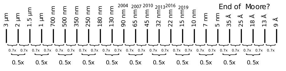
Table from wikichip.org [Ref. #2]
While production is currently in the size range where some effects of nanomaterials can occur, more impact is coming shortly. The semiconductor industry is working on many different options including three-D stacking and innovative designs for transistors. However, the projection is still to go to smaller and smaller sizes with the increasing challenges. The last two blogs have provided some thoughts on the challenges.
There are numerous “surprises” with nanomaterials. The fact that non-magnetic material can have magnetic properties at 13 atoms is interesting. I am unaware of anyone who is investigating that property in incorporate in an application. Transition metal in five different states: as hydrated atom; metal complexed in a small protein; metal adsorbed to surface on 1nm mineral particle; metal adsorbed to surface of 20nm particle; the same except to a 200nm particle. [Ref. #3] In addition, size may matter for crystal orientation preferences. For example, CeO2 < 10nm prefers being a truncated octahedron with {100} and {111} faces. CeO2 > 10nm shifts toward {111} octahedron. [Ref. #4]
So, what is going to be done? There are many different portions to solving the problem. Consider the time it takes a signal to cross from one side of a semiconductor chip to the other side. How can the timing be maintained? One possibility is to use light. This requires some type of light guide on the semiconductor. Research in this area has been ongoing for many years. Recently there have been some initial publications of employing two dimensional material, like graphene, to create tunable gratings on the nano scale. Is that where semiconductors are going? Not in the near future, but it is one possible avenue of research for smaller and faster circuitry.
One item that has not been mentioned is the fact that at small scale, circuitry tends to increase the amount of energy lost, especially as heat. As the computing power increases, the amount of heat generated increases. As the amount of power required increases, the size of the power supply increases. That makes portable electronics a problem. While there is work ongoing to improve the capacity of batteries, the improvements have not experienced any breakthroughs. A number of published articles have demonstrated advances by carefully controlling the nanomaterials employed in the battery.
The above is just a few of the potential challenges for the future. The manufacturing challenges have not been mentioned, but they are substantial. The development of increased capability electronics will witness learning more about and how to properly incorporate nanomaterials in a manner that improves performance and decreases the proportional power requirements.
References:
- https://spectrum.ieee.org/semiconductors/design/shrinking-possibilities
- https://en.wikichip.org/wiki/technology_node
- Hochella, Michael F. Jr.. Nanogeoscience: From Origins to Cutting Edge Applications. December 2008 issue. Vol. 4, pp. 373-379.
- Waychunas, Glenn A., Hengzhong Zhang. Structure, Chemistry, and Properties of Mineral Nanoparticles. December 2008 issue. Elements. 4, pp381-387.