
The design of the semiconductor circuit components has been evolving as the feature size shrinks. The semiconductor industry has been able to develop new designs as older techniques become restrictive due to various material properties. This blog is a short review of the history of development of device structures with some thoughts on the coming changes. There were many different types of transistors during the 1950s, 1960s, and into the 1970s. These can be found in many places on-line, including Wikipedia [Ref. 1].
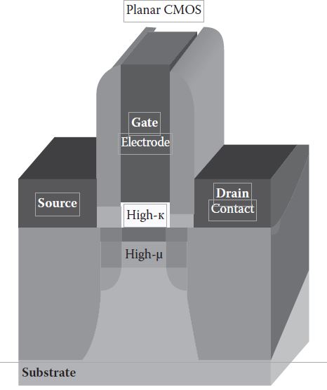
The field effect transistor (FET) has been a staple of semiconductor manufacturing for years. The majority of the devices produced through the 2000s were complementary metal-oxide-semiconductors (CMOS). The picture below, from reference #2 shows the components of the FET.
The manufacture of FETs are directly ono the silicon wafers. The gate electrode is the control for the flow of the charges, either electrons or holes. The structure is structured with planar layers, which gives rise to the term “planar gate”. As the size of the semiconductor components, the dimensions became smaller. The shrinkage of the gate length increased the switching speed with the result faster electronics. Problems began to arise as the gate length shrunk toward 20nm. The current could flow without any control by the gate electrode.
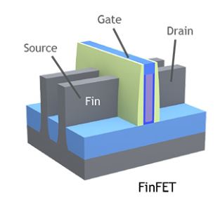
The issue of not having enough surface area to control the FET was addressed with the development of the FinFET. The picture below is from reference #3. The gate material is vertical and provides more volume for controlling the flow of the charge. The “source” and “drain” are also vertical (fins) that provide a better control that operates at a lower voltage, which also provides better performance. Unfortunately, the design is more complex and challenging to produce. Semiconductor manufacturing has kept up with these challenges, but …..
With the current view of the future of production, FinFET are starting to reach their limit. So, a different solution needs to be developed. There are some thoughts about increasing the “fins” to cover more contact area. This is shown below as the Gate-All-Around FET [Ref. 4]. Others are looking at different designs. The Multi-bridge Channel FET was identified in the early 2000s, but manufacturing technology was not available.
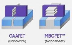
The development of the GAAFET was led by IBM. Samsung has move beyond the collaboration to the MBCFET, which it contends will be in production for the 3nm node.
There are challenges to gate-all-around designs. There is only modest improvement over FinFets at 5nm. The manufacturing technology is challenging [Ref. 6] with tighter manufacturing requirements due to greater complexity. The current version of the devices requires a silicon, silicon-germanium, and silicon super lattice stack. More details of the process is available in reference 6. The projection is for the introduction on the GaaFET at 3nm.
Historically, each succeeding node brings with it move transistors per unit area with lower power and higher performance at a lower cost per transistor. Due to the greater challenges in producing the smaller and smaller transistors, that fact is no longer true. The question I s not whether or not the technology will continue to advance, but how will the technology transform to continue to provide more capable devices.
References:
- https://en.wikipedia.org/wiki/Transistor
- Chapter 2: Nanotechnology in Electronics, Larry Larson et al, Nanotechnology for Sustainable Manufacturing. Pp. 17-35. CRC Press. David Rickerby editor. 2016. ISBN13: 978-1-4822-1483-3
- https://blog.lamresearch.com/tech-brief-finfet-fundamentals/
- https://www.pcgamesn.com/samsung/3nm-gaa-beat-tsmc
- https://wccftech.com/samsung-announces-3nm-mbcfet-process-5nm-production-in-2020/
- https://semiengineering.com/5nm-vs-3nm/